Stripping and removal of organic-containing materials from electronic device substrate surfaces
a technology of electronic devices and substrate surfaces, applied in the direction of photomechanical equipment, instruments, cleaning using liquids, etc., can solve the problems of unacceptably slow removal rate of organic materials, reduce the solubility of ozone in the stripping solution, and reduce the odor of the stripping solution and minor corrosion
- Summary
- Abstract
- Description
- Claims
- Application Information
AI Technical Summary
Benefits of technology
Problems solved by technology
Method used
Image
Examples
example one
Removal of Photoresist from a Substrate Surface Using Ozonated Acetic Anhydride
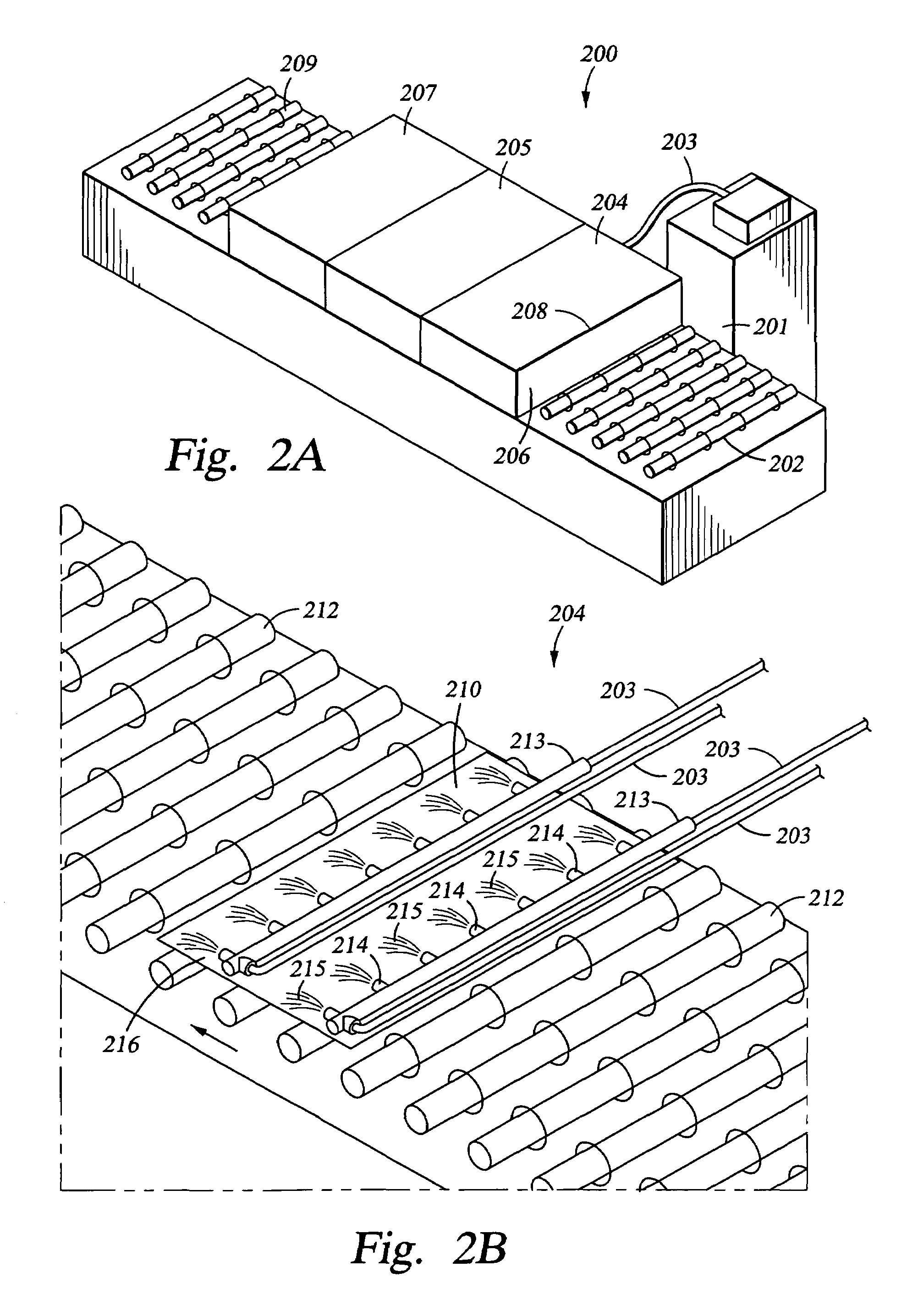
[0080]A layer of a deep ultra-violet (DUV) photoresist which is sensitive to 248 nm radiation (UV 6, available from Shipley, Marlborough, Mass.) was applied to a thickness of approximately 10,000 Å (1,000 nm) onto the surface of a single-crystal silicon wafer. The photoresist was applied using a spin-on process, then baked for 30 minutes at 95° C. Ozonated acetic anhydride (100% acetic anhydride) stripping solution containing about 300 ppm (mg / L) of ozone was sprayed onto the surface of the photoresist-coated substrate at room temperature (25° C.) using a dispensing system such as that shown in FIG. 2B. The ozonated acetic anhydride was allowed to react with the photoresist for a period of 30, 60, or 120 seconds, then rinsed off the substrate surface by spraying with deionized water for a period of 10 to 20 seconds.
[0081]A series of six substrate samples were tested, where 1 μm of photoresist was present ...
example two
Corrosivity of Ozonated Acetic Anhydride on Aluminum
[0082]A layer of aluminum was deposited to a thickness of about 10,000 Å onto the surface of a single-crystal silicon wafer using a physical vapor deposition (PVD) process of the kind known in the art. To test the corrosivity of ozonated acetic anhydride stripping solution on aluminum, ozonated acetic anhydride (100% acetic anhydride) stripping solution containing about 300 ppm (or mg / L) of ozone was sprayed onto the surface of the aluminum-coated substrate at room temperature (25° C.) using a dispensing system such as that shown in FIG. 2B. The ozonated acetic anhydride stripping solution was allowed to react with the aluminum for a period of 30, 60, or 120 seconds, then rinsed off the substrate surface by spraying with deionized water for a period of 10 to 20 seconds.
[0083]Within the accuracy of our ability to measure, aluminum was not removed by the ozonated acetic anhydride stripping solution. There appears to be a slight incre...
example three
Corrosivity of Ozonated Acetic Anhydride a Copper Surface
[0084]A layer of copper was deposited to a thickness of 8,000 Å (800 nm) to 19,000 Å (1,900 nm) onto the surface of a single-crystal silicon wafer. The copper was deposited using a physical vapor deposition (PVD) process, followed by electrochemical plating. In order to test the corrosivity of ozonated acetic anhydride stripping solution on copper, ozonated acetic anhydride (100% acetic anhydride) containing at least 300 ppm (or mg / L) of ozone was sprayed onto the surface of the copper-coated substrate at room temperature (25° C.) using a dispensing system such as that shown in FIG. 2B. The ozonated acetic anhydride stripping solution was allowed to react with the copper surface for a period of 30, 60, or 120 seconds, then rinsed off the substrate surface by spraying with deionized water for a period of 10 to 20 seconds.
[0085]Table Four, below, shows the thickness of the titanium nitride layer before and after treatment with a...
PUM
| Property | Measurement | Unit |
|---|---|---|
| temperature | aaaaa | aaaaa |
| temperature | aaaaa | aaaaa |
| area | aaaaa | aaaaa |
Abstract
Description
Claims
Application Information
 - R&D
- Intellectual Property
- Life Sciences
- Materials
- Tech Scout
- Unparalleled Data Quality
- Higher Quality Content
- 60% Fewer Hallucinations
Browse by: Latest US Patents, China's latest patents, Technical Efficacy Thesaurus, Application Domain, Technology Topic, Popular Technical Reports.
© 2025 PatSnap. All rights reserved.Legal|Privacy policy|Modern Slavery Act Transparency Statement|Sitemap|About US| Contact US: help@patsnap.com


