Apparatus and method for improved triggering and oscillation suppression of ESD clamping devices

a technology of esd clamping device and apparatus, which is applied in the field of electrostatic discharge, can solve the problems of low power requirements, esd events becoming particularly troublesome for complementary metal oxide semiconductor (cmos) chips, and substantial damage to the i

Inactive Publication Date: 2008-07-08
IBM CORP
View PDF16 Cites 11 Cited by
  • Summary
  • Abstract
  • Description
  • Claims
  • Application Information

AI Technical Summary

Benefits of technology

[0006]The foregoing discussed drawbacks and deficiencies of the prior art are overcome or alleviated by an apparatus for protecting an integrated circuit from electrostatic discharge (ESD). In an exemplary embodiment, the apparatus includes an RC trigger device configured between a pair of power rails, a first control path coupled to the RC trigger device, and a second control path coupled to the RC trigger device. A power clamp is configured between the power rails for discharging current from an ESD event, the power clamp having an input coupled to outputs of the first and second control paths, the power clamp independently controllable by the first and second control paths. The first and second control paths are further configured to prevent the power clamp from reactivating following an initial deactivation of the power clamp.
[0007]In another embodiment, a method for protecting an integrated circuit from electrostatic discharge (ESD) includes configuring an RC trigger device between a pair of power rails and coupling first and second control paths to the RC trigger device. A power clamp is configured between the power rails for discharging current from an ESD event, said power clamp having an input coupled to outputs of the first and second control paths, the power clamp independently controllable by the first and second control paths. The first and second control paths are further configured to prevent the power clamp from reactivating following an initial deactivation of the power clamp.

Problems solved by technology

ESD events, which can occur both during and after manufacturing of an integrated circuit (IC), can cause substantial damage to the IC.
ESD events have become particularly troublesome for complementary metal oxide semiconductor (CMOS) chips because of their low power requirements and extreme sensitivity.
When a transistor is exposed to an ESD event, the charge applied may cause an extremely high current flow to occur within the device, which in turn can cause permanent damage to the junctions, neighboring gate oxides, interconnects and / or other physical structures.
The continued scaling of semiconductor devices has resulted in some unique challenges for providing ESD protection in CMOS applications.
Unfortunately, existing circuit topologies that provide sufficient ESD protection do not also prevent oscillation of the ESD power clamps as a result of the interaction of high transient current with the package inductance / resistance of the package.

Method used


Image

  • Apparatus and method for improved triggering and oscillation suppression of ESD clamping devices
  • Apparatus and method for improved triggering and oscillation suppression of ESD clamping devices
  • Apparatus and method for improved triggering and oscillation suppression of ESD clamping devices

Examples


Embodiment Construction

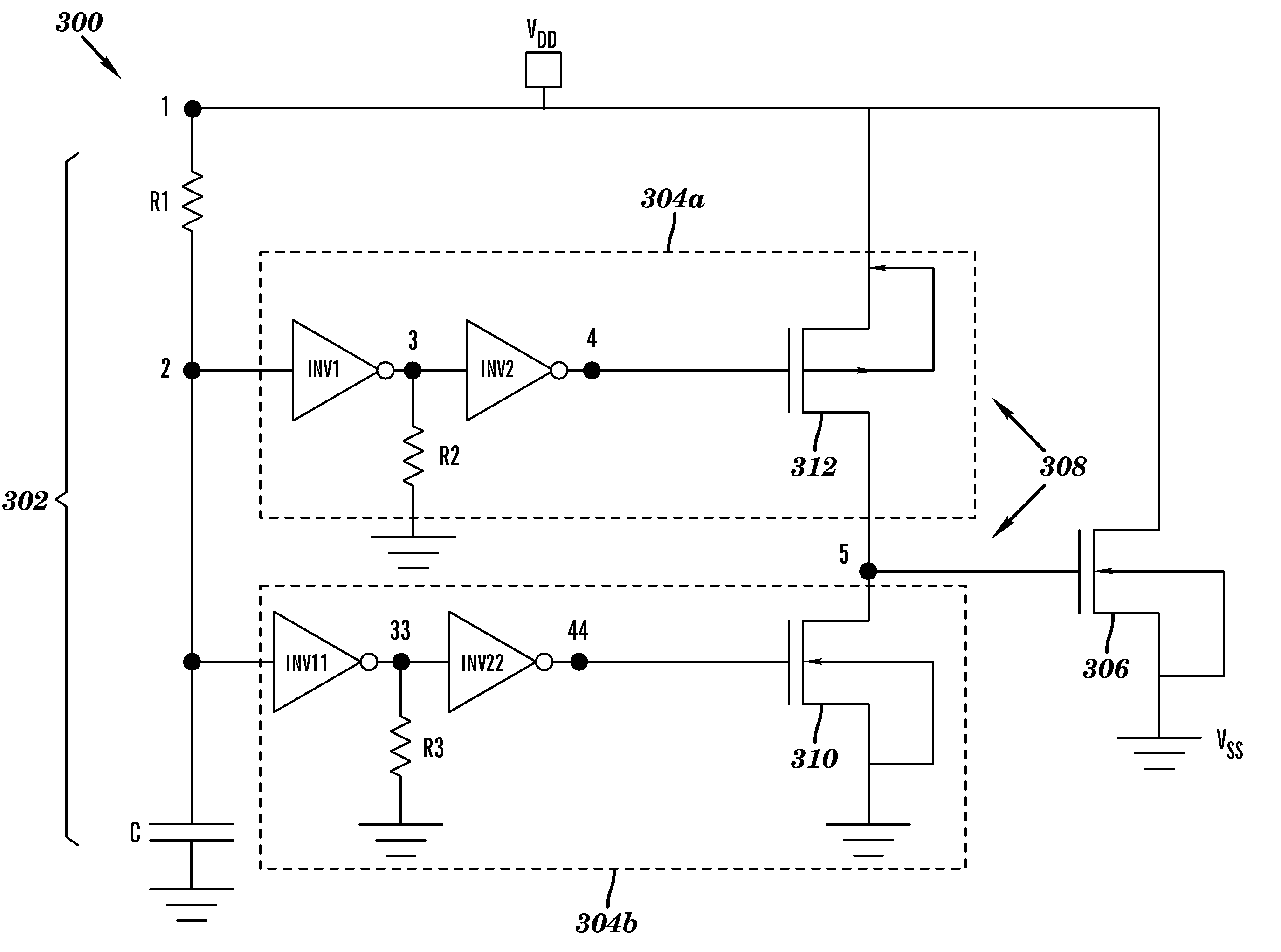
[0012]Disclosed herein is an apparatus and method for improved triggering and oscillation suppression of electrostatic discharge (ESD) power clamping devices. Briefly stated, separate inverter stages are used in an ESD protection circuit to provide a first and a second control path with respect to a FET clamp. By using independent inverter stages with different switch points, the problem of power rail oscillations during fast power-up conditions is eliminated. Additional advantages of the embodiments presented herein will also become apparent.

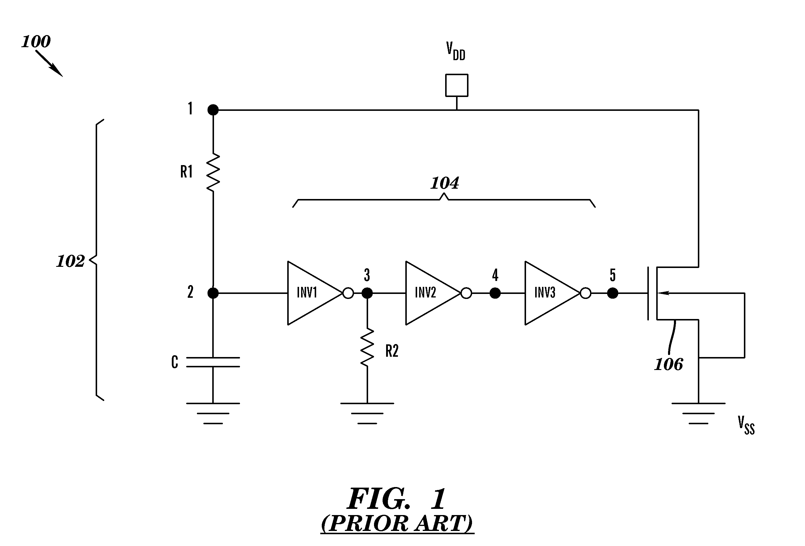
[0013]Referring initially to FIG. 1, there is shown a schematic diagram of an existing ESD clamp circuit 100 configured between a pair of power rails. In the example illustrated, the rails are shown as nominally being powered by VDD and ground potential. However, the clamp 100 may also be configured between power rails of different voltage levels (e.g., VDDX and VDDY), as well as between ground and VSS (negative potential), for example. As is w...


PUM


Abstract

An apparatus for protecting an integrated circuit from electrostatic discharge (ESD) includes an RC trigger device configured between a pair of power rails, a first control path coupled to the RC trigger device, and a second control path coupled to the RC trigger device. A power clamp is configured between the power rails for discharging current from an ESD event, the power clamp having an input coupled to outputs of the first and second control paths, the power clamp independently controllable by the first and second control paths. The first and second control paths are further configured to prevent the power clamp from reactivating following an initial deactivation of the power clamp.

Description

BACKGROUND[0001]The present invention relates generally to electrostatic discharge (ESD) in integrated circuits, and, more particularly, to an apparatus and method for improved triggering and oscillation suppression of ESD power clamping devices.[0002]ESD events, which can occur both during and after manufacturing of an integrated circuit (IC), can cause substantial damage to the IC. ESD events have become particularly troublesome for complementary metal oxide semiconductor (CMOS) chips because of their low power requirements and extreme sensitivity. A significant factor contributing to this sensitivity to ESD is that the transistors of the circuits are formed from small regions of N-type materials, P-type materials, and thin gate oxides. When a transistor is exposed to an ESD event, the charge applied may cause an extremely high current flow to occur within the device, which in turn can cause permanent damage to the junctions, neighboring gate oxides, interconnects and / or other phy...

Claims


Application Information

Patent Timeline
Patent Type & Authority Patents(United States)
IPC IPC(8): H02H9/00H02H1/00
CPCH01L27/0266
Inventor CHU, ALBERT M.GAUTHIER, JR., ROBERT J.LI, JUNJUNWYCKOFF, THOMAS W.
Owner IBM CORP
Why Eureka
Try Eureka