
Method for optimizing the performance of a semiconductor detector

a technology of semiconductor detectors and optimization methods, which is applied in the field of x-rays and -rays, can solve the problems of native flaws that cannot be avoided, the use of semiconductor materials poses a technical problem, and the hole is difficult to reach the electrodes and, especially, the cathode, so as to facilitate the optimization of the spatial resolution of such a detector

Active Publication Date: 2008-05-27
COMMISSARIAT A LENERGIE ATOMIQUE ET AUX ENERGIES ALTERNATIVES
View PDF3 Cites 7 Cited by
  • Summary
  • Abstract
  • Description
  • Claims
  • Application Information

AI Technical Summary

Benefits of technology

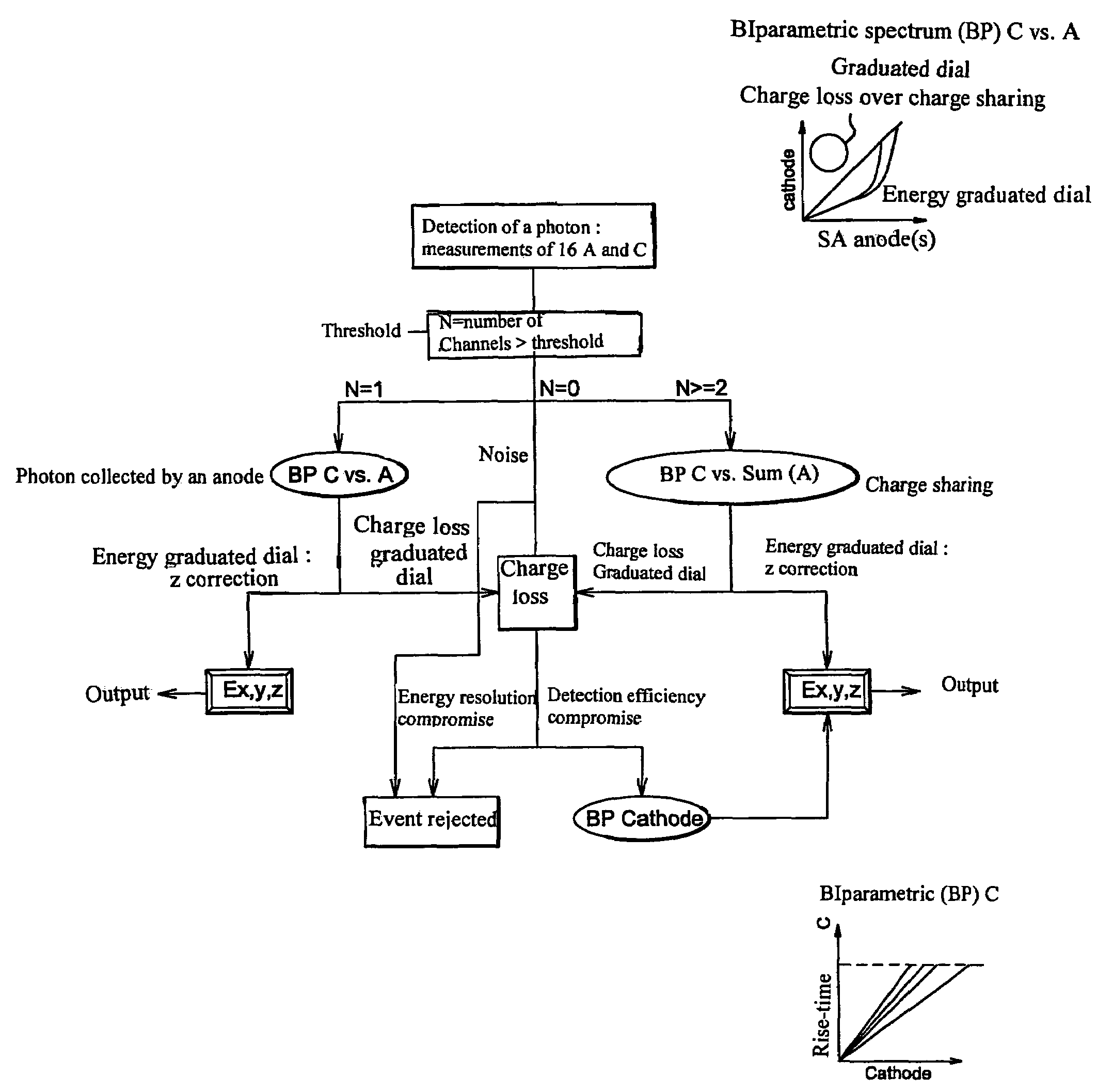
[0044]The object of the present invention is to integrate these various data whilst retaining the principle of reducing the dimensions of the anode pixels which, as will be readily understood, facilitates optimizing the spatial resolution of such a detector.
[0057]In an attempt to reduce the inherent noise of the measurement process, for each event, i.e. for each incident photon, one determines the signal induced on each anode and on the cathode and one compares these signals to a respective predefined energy threshold, beyond which the event in question is ignored.
[0061]In the second case, one extracts the total energy that corresponds to this particular event from the biparametric spectrum that corresponds to the signal for the rise-time of the cathode signal (TC) as a function of the signal that corresponds to the amplitude of the cathode (C) in order to take it into account when restoring the final spectrum, and subsequently, in order to preserve detection efficiency.

Problems solved by technology

When it comes to energy resolution, using a semiconductor material poses a technical problem that is inherent to the material itself.
Despite the progress made in growing crystals, such native flaws cannot currently be avoided.
For example, in a semiconductor detector based on CdZnTe, holes find it difficult to reach the electrodes and, especially, the cathode.
On the one hand, this problem of incomplete collection degrades energy resolution, and, on the other hand, also reduces collection efficiency for a given energy.
Nevertheless, it should be noted that this “pixel effect” has two paradoxical characteristics:an imaging system that uses the above-mentioned detector may impose an optimized spatial resolution, and hence a pixel pitch, especially that of the anode, which is not necessarily compatible with efficient correction using the “pixel effect”;the above-mentioned imaging system may impose a performance, in terms of energy resolution and hence an anode pixel pitch, which is not necessarily compatible with the spatial resolution of the expected system.
In contrast, using such a biparametric spectrum does pose one difficulty: measuring an anode signal rise-time that is accentuated as the pitch of the pixelated anode reduces.
In contrast, using such spectra has the inherent drawback that the cathode signal very quickly becomes noisy if its surface area is large, i.e. in the case of monolithic detectors having large dimensions.
However, because of the increasingly high performance-requirements placed on detectors, there is pressure to reduce the size of the pixels still further, especially on the anode, and this results in the occurrence of a phenomenon that has a tendency to become more marked: charge sharing which results in deterioration of overall performance of the detector despite using the said techniques.
The smaller the dimensions of the anodes, the worse this charge-sharing problem becomes.
However, this summing does not necessarily correspond to energy of the photons if, because of the difference between surface conductivity and volume conductivity and / or because of trapping of charges close to the surface, charges are actually lost and the sum of the amplitudes remains less than the energy of the absorbed photons.
Regardless of the situation with this alternative, there still remains the problem that the measured charge is dependent on the interaction depth.

Method used


Image

  • Method for optimizing the performance of a semiconductor detector
  • Method for optimizing the performance of a semiconductor detector
  • Method for optimizing the performance of a semiconductor detector

Examples


Embodiment Construction

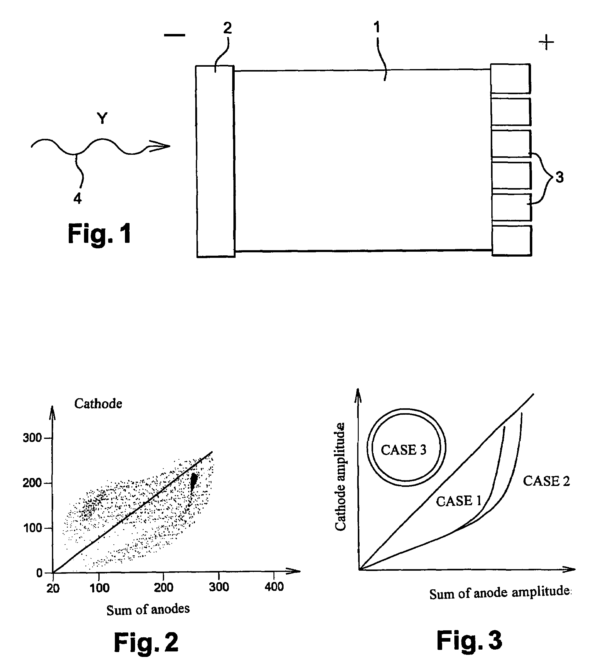
[0071]A semiconductor detector as implemented by the present invention is described very succinctly, reference being made to FIG. 1. It comprises a solid semiconductor 1 produced, for example, by crystal growth, made of CdZnTe or CdTe for instance. These materials are currently well known for their ability to convert the energy resulting from an X or γ photon 4 into an electron / hole charge pair.

[0072]Electrodes, a cathode 2 and anode 3 respectively, are separately mounted on the two main opposite surfaces of semiconductor 1. One then applies a bias voltage to the semiconductor making it possible to ensure migration of the charges generated following interaction between photon 4 and semiconductor 1.

[0073]In addition, on each of the electrodes, one measures a signal, the amplitude of which directly correlates to the quantity of charges thus generated.

[0074]Anode 3 is pixelated, one of the objectives of the present dimension being to reduce the dimension of the pixels or the inter-pixe...


PUM


Abstract

This method for optimizing the performance of a semiconductor detector intended to detect electromagnetic radiation, especially X-rays or γ rays, equipped with electrodes separately mounted on two opposite surfaces of said detector, namely a cathode and a pixelated anode respectively, involves (i) determining the signal that is representative of the sum of the charges detected by all or some of the anodes; and (ii) using the signal that is representative of said sum of the charges to establish one or more biparametric spectra as a function of this signal so as to determine any charge collection loss if charge sharing occurred on the pixelated anodes and, consequently, performing appropriate processing depending on the type of result desired.

Description

FIELD OF INVENTION[0001]The present invention relates to the field of detecting electromagnetic radiation, especially X-rays and γ rays. The invention uses a semiconductor detector.[0002]More especially, the invention concerns the field of medical and scientific imaging as well as non-destructive tests on structures and the field of security (detection of prohibited or controlled products in baggage and carried by passengers).[0003]Overall, the invention relates to the detection of electromagnetic radiation making it possible to combine high energy resolution performance with equally high spatial resolution performance.DESCRIPTION OF THE PRIOR ART[0004]The use of semiconductor detectors in the context of detecting electromagnetic radiation is now well-known. Such detectors directly convert incident radiation into energy without having to use any intermediate steps of the visible photon emission type that is familiar in the field of scintillators.[0005]In addition, the energy require...

Claims


Application Information

Patent Timeline
Patent Type & Authority Patents(United States)
IPC IPC(8): G01T1/24
CPCG01T1/17G01T1/2928
Inventor GROS D'AILLON, ERICVERGER, LOICK
Owner COMMISSARIAT A LENERGIE ATOMIQUE ET AUX ENERGIES ALTERNATIVES
Learn More