Mobile communication apparatus
a communication device and mobile technology, applied in transmission, substation equipment, pulse technique, etc., can solve the problems of difficult to cancel the dc offset, difficult to anticipate the dc offset voltage, and unsuitable for high-speed data communications, etc., to achieve the effect of fast cancellation of the dc offs
- Summary
- Abstract
- Description
- Claims
- Application Information
AI Technical Summary
Benefits of technology
Problems solved by technology
Method used
Image
Examples
second embodiment
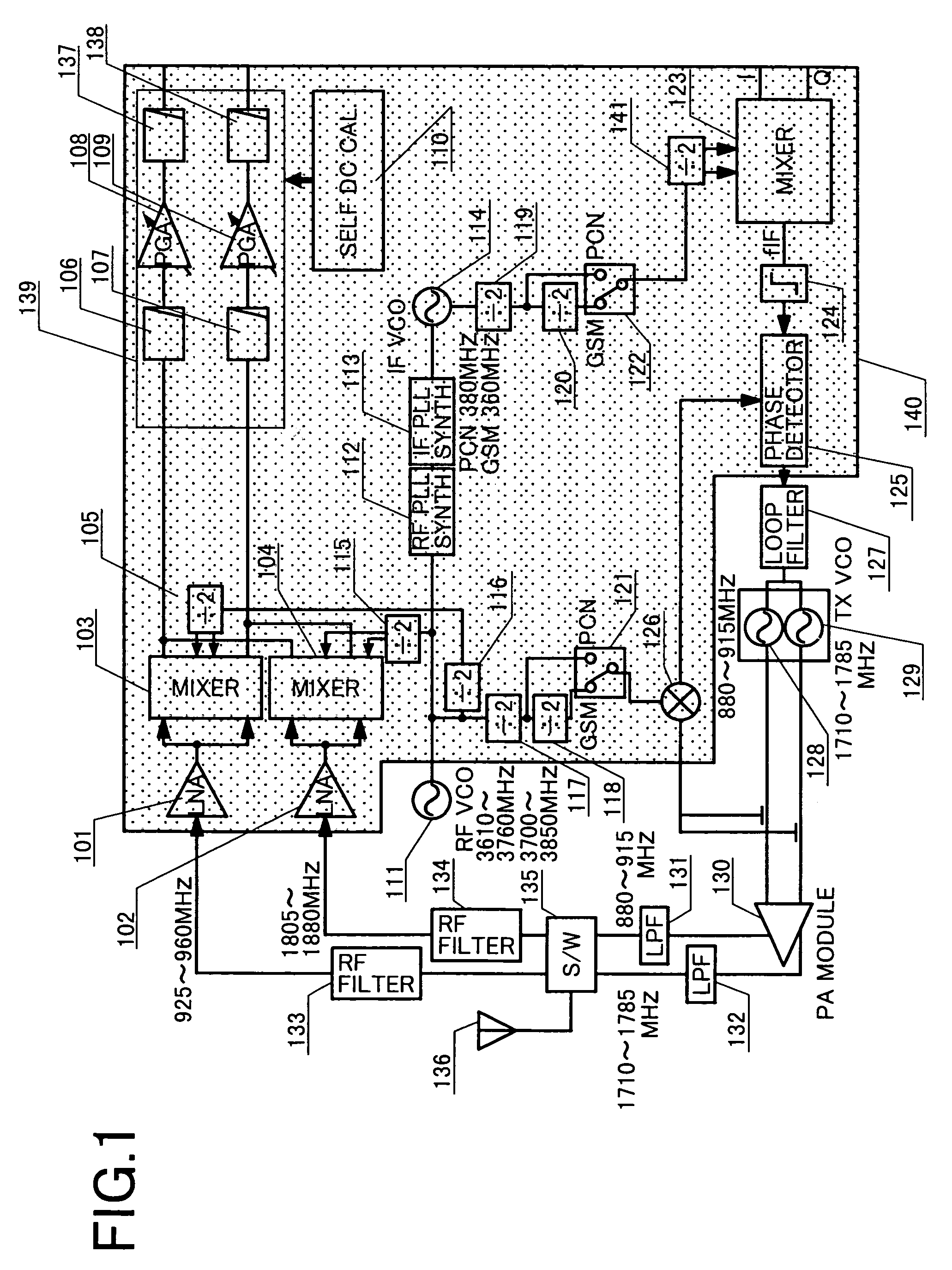
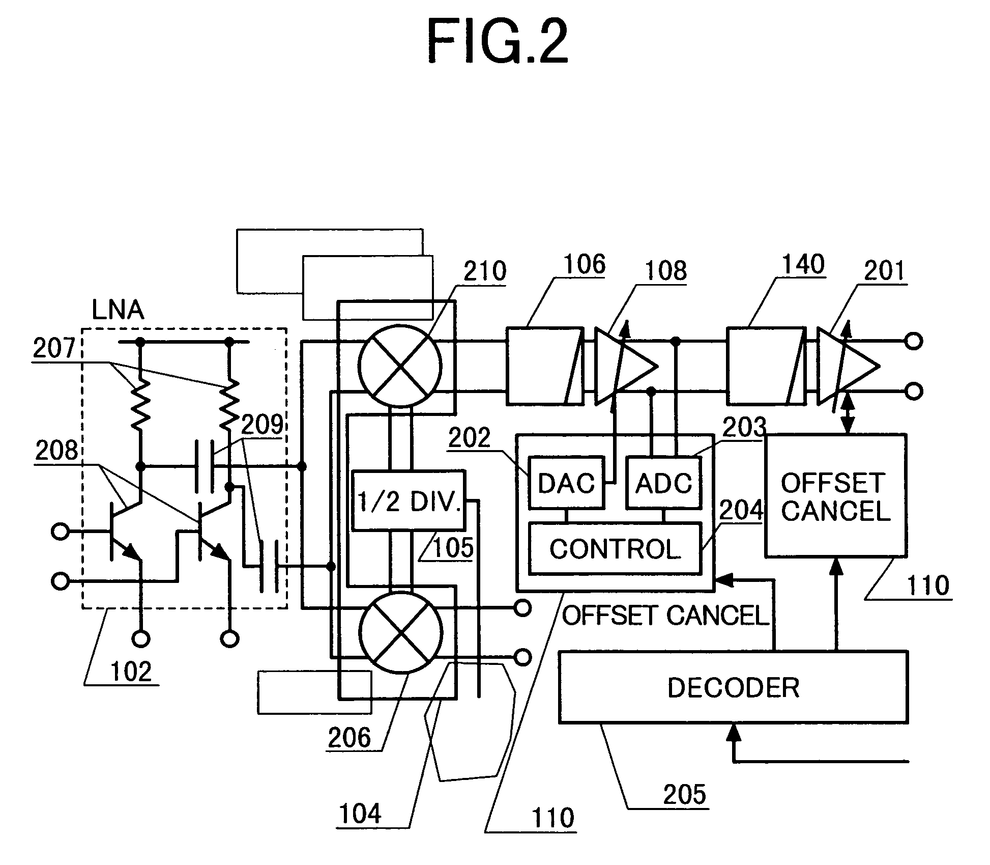
[0045]Next, a receiver according to the present invention will be described with reference to FIG. 2.
[0046]The illustrated receiver comprises a low noise amplifier 102; a mixer 104; a divider 105; low pass filters 106, 137; variable gain amplifiers 108, 201; DC offset voltage canceling circuits 110; and a decoder 205. The low noise amplifier 102 in turn comprises a load resistor 207; a transistor 208; and a capacitance 209, while the DC offset voltage canceling circuit 110 comprises a digital-to-analog converter (DAC) 202; an analog-to-digital converter (ADC) 203; and a controller 204. The mixer 104 comprises mixers 210, 206.
[0047]An output DC voltage of the variable gain amplifier 108 is converted to a digital signal by the ADC 203, and inputted to the controller 204. The controller 204 measures the DC offset voltage at the output of the variable gain amplifier 108 to output a cancel signal for canceling the DC offset voltage. The cancel signal is converted from a digital signal to...
third embodiment
[0048]Next, a variable gain amplifier and a DC offset voltage canceling circuit according to the present invention will be described with reference to FIG. 3.
[0049]The variable gain amplifier comprises resistors 307, 308, 312; and transistors 309, 310, 311. The transistors 309, 310 are applied with an input voltage at their bases to deliver output voltages from their collectors. The gain can be controlled, for example, by a base voltage of the transistor 311. A DAC 313 comprises transistors 301, 302, 303; and resistors 304, 305, 306. Since the output of a controller 204 is connected to bases of the transistors 301, 302, 303, the controller 204 can control collector DC currents of the transistors 301, 302, 303. The collector DC currents are summed with a collector current of the transistor 309, and then converted to a voltage by the resistor 307. Assume now that a DC offset voltage ΔV (=V2−V1) exists, and the resistance of the resistors 307, 308 are represented by RL; an output DC cu...
PUM
 Abstract
Description
Claims
Application Information
 - R&D
- Intellectual Property
- Life Sciences
- Materials
- Tech Scout
- Unparalleled Data Quality
- Higher Quality Content
- 60% Fewer Hallucinations
Browse by: Latest US Patents, China's latest patents, Technical Efficacy Thesaurus, Application Domain, Technology Topic, Popular Technical Reports.
© 2025 PatSnap. All rights reserved.Legal|Privacy policy|Modern Slavery Act Transparency Statement|Sitemap|About US| Contact US: help@patsnap.com


