Memory array with global bitline domino read/write scheme

a memory array and domino technology, applied in the field of electronic systems, can solve the problems of erroneous reading/writing of memory cells, slow operation speed, and inconvenient traditional arrangement shown abov

Inactive Publication Date: 2008-04-08
ADVANCED SILICON TECH
View PDF11 Cites 14 Cited by
  • Summary
  • Abstract
  • Description
  • Claims
  • Application Information

AI Technical Summary

Benefits of technology

[0010]The memory circuit may be part of a memory subsystem. The memory subsystem may include a control circuit, which provides signals for reading, writing, and precharging to the memory arrays. The control circuit may further control the sequence in which reading, writing, and precharging is performed, and may further control which of these operations are performed for a given memory cycle.

Problems solved by technology

With the advent of smaller feature sizes in current microprocessors (and other types of integrated circuits), the trend towards lower operating voltages, and the increases in operating speed (i.e. clock frequencies), the traditional arrangement shown above may not always be suitable.
These biases, in the absence of compensation, may cause erroneous values to be read from the memory cells.
However, even this approach may suffer some of the same drawbacks as the previous approach with the aforementioned advent of smaller feature sizes, lower operating voltages, and increases in operating speed.
Thus, these circuit designs may be inadequate for newer microprocessors or other circuits which implement memory circuits as shown in FIG. 1.

Method used


Image

  • Memory array with global bitline domino read/write scheme
  • Memory array with global bitline domino read/write scheme
  • Memory array with global bitline domino read/write scheme

Examples


Embodiment Construction

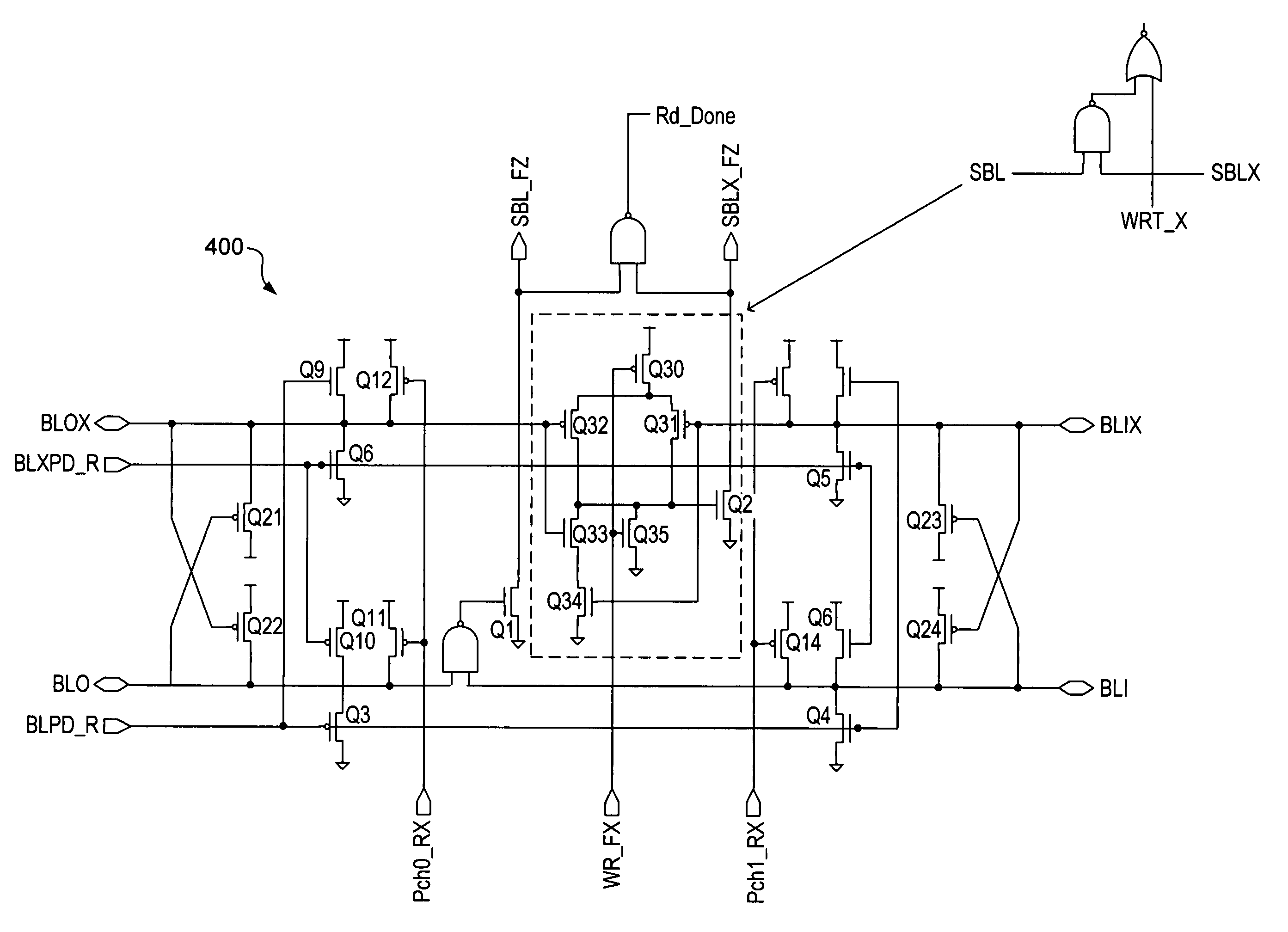
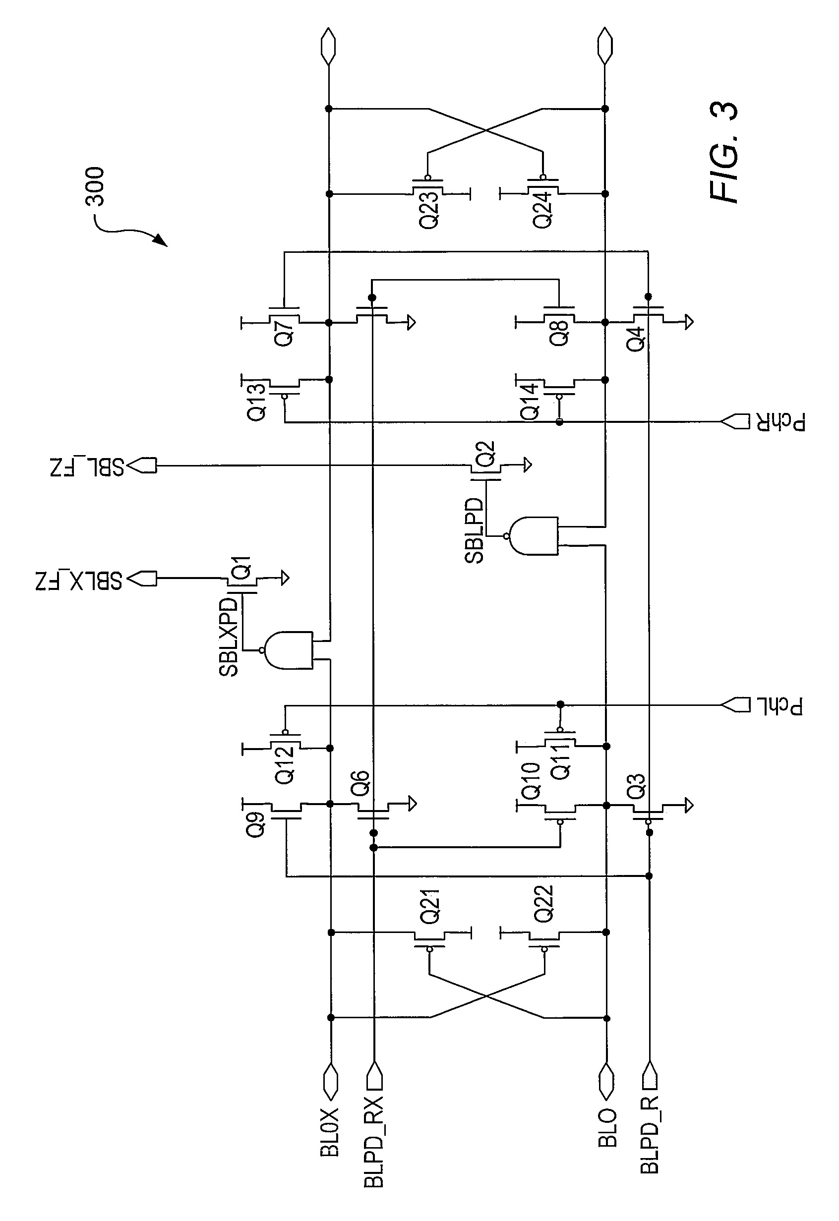
[0022]Turning now to FIG. 3, a schematic diagram of one embodiment of circuit for a memory array wherein the circuit includes local bitlines coupled to a global bitline is shown. The circuit may be used in a memory circuit that uses a global bitline domino read / write scheme.

[0023]In the embodiment shown, circuit 300 includes a first differential local bitline pair (BL0, BL0X) and a second differential local bitline pair (BL1, BL1X). Each of the bitline pairs is coupled to a plurality of memory cells (not shown here). The local bitline pairs are each operatively coupled to a global (or super) bitline in domino scheme arrangement. In this particular example, each of the local bitlines are coupled to inputs of a NAND gate, with the NAND gate output coupled to the gate terminal of a transistor (n-channel in this case) which is coupled to pull down the global bitline when active. Both of BL0X and BL1X are coupled to one of the NAND gates, which in turn is operatively coupled to global bi...


PUM


Abstract

A circuit for implementing memory arrays using a global bitline domino read / write scheme. The memory circuit includes a plurality of cells each configured to store a bit of data. The memory circuit further includes a plurality of local bitlines, wherein each cells is coupled to one of the local bitlines. Each of the plurality of local bitlines is a differential bitline having a signal path and a complementary signal path which are cross-coupled by a pair of transistors.

Description

BACKGROUND OF THE INVENTION[0001]1. Field of the Invention[0002]This invention relates to electronic systems, and more particularly, circuitry for addressing memory devices in electronic systems.[0003]2. Description of the Related Art[0004]Memories such as cache memories include a plurality of cells arranged in an array. The cells may be connected to each other by bitlines and wordlines. One embodiment of an array of cells in a cache memory is shown in FIG. 1. As shown in the drawing, the cells are connected in rows by wordlines and connected in columns by pairs of bitlines. Each bitline of a plurality of cells may convey a signal that is a logical complement with respect to the signal carried on the other bitline of the pair (which may be referred to as an inverse bitline). Sense amplifiers may be coupled to the bitlines in order to amplify and transmit signals received therefrom.[0005]With the advent of smaller feature sizes in current microprocessors (and other types of integrate...

Claims


Application Information

Patent Timeline
Patent Type & Authority Patents(United States)
IPC IPC(8): G11C11/00G11C7/00G11C7/10
CPCG11C7/1057G11C7/12G11C7/18G11C7/1051G11C2207/002
Inventor DANKERT, FLOYD L.ANDRADE, VICTOR F.POSEY, RANDAL L.CIRAULA, MICHAEL K.SCHAEFER, ALEXANDER W.MOENCH, JERRY D.CHRUDIMSKY, SOOLIN KAOBRAGANZA, MICHAEL C.HUBER, JAN MICHAELNOVAK, AMY M.
Owner ADVANCED SILICON TECH
Why Eureka
Try Eureka