Scan based automatic test pattern generation (ATPG) test circuit, test method using the test circuit, and scan chain reordering method

an automatic test pattern and test circuit technology, applied in the field of semiconductor chip testing methods, can solve the problems of excessive test time required by the above method, large amount of test data required, and test tim

Active Publication Date: 2008-03-11
SAMSUNG ELECTRONICS CO LTD
View PDF8 Cites 9 Cited by
  • Summary
  • Abstract
  • Description
  • Claims
  • Application Information

AI Technical Summary

Benefits of technology

[0024]Embodiments of the invention provides a scan based ATPG test circuit capable of testing and diagnosing a plurality of scan chains while preventing unknown values that exist in the scan chains from influencing a test result.
[0025]Embodiments of the invention also provides a scan chain reordering method capable of testing and diagnosing a plurality of scan chains while preventing unknown values that exist in the scan chains from influencing a test result.

Problems solved by technology

The amount of test time required by the above method is excessive and hence a method requiring less test time is desired.
Testing a highly integrated device such as a SOC using the conventional ATPG structure shown in FIG. 1 requires verification of an enormous amount of test data compared with testing general semiconductor devices.
Because the ATE has a limited memory capacity, this causes a significant increase in test costs.
However, where an error is generated in a second cycle of second scan chain SCAN CHAIN #2 and simultaneously an unknown value (hereinafter, referred to as X) exists in a second cycle of the third scan chain SCAN CHAIN #3, a problem arises.
However, this approach has problems in that it creates design / implementation overhead and it requires further implementations and verifications anytime the design is revised.

Method used


Image

  • Scan based automatic test pattern generation (ATPG) test circuit, test method using the test circuit, and scan chain reordering method
  • Scan based automatic test pattern generation (ATPG) test circuit, test method using the test circuit, and scan chain reordering method
  • Scan based automatic test pattern generation (ATPG) test circuit, test method using the test circuit, and scan chain reordering method

Examples


Embodiment Construction

[0040]The invention will now be described more fully with reference to the accompanying drawings in which several embodiments of the invention are shown.

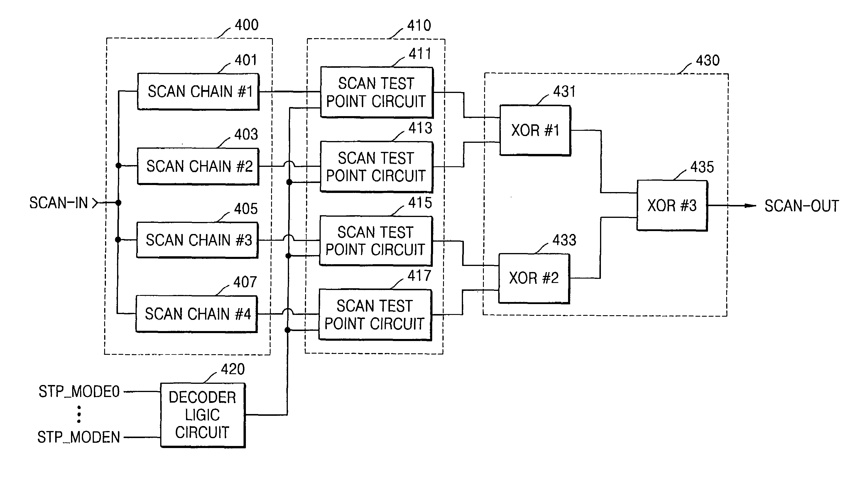
[0041]FIG. 4 is a diagram showing a scan based ATPG test circuit according to one embodiment of the invention.

[0042]Referring to FIG. 4, the scan based ATPG test circuit comprises a scan input pin SCAN_IN, a scan chain group 400, a scan test point group 410, a decoder logic circuit 420, a scan test data compressor 430, and a scan output pin SCAN-OUT. Test data generated by ATPG is received through scan input pin SCAN-IN.

[0043]Scan chain group 400 comprises first through fourth scan chains 401, 403, 405, and 407, also respectively called SCAN CHAIN #1 through SCAN CHAIN #4. First through fourth scan chains 401, 403, 405, and 407 are chains of test sources connected according to a predetermined rule.

[0044]Scan test point group 410 comprises first through fourth scan test point circuits 411, 413, 415, and 417. Each scan test point circ...


PUM


Abstract

A scan based Automatic Test Pattern Generation (ATPG) test circuit, a test method using the test method, and a scan chain reordering method are disclosed. The test circuit tests for scan chains comprising unknown values which could adversely influence a test result. The test circuit uses a scan test point circuit to prevent unknown values from propagating through the test circuit, thus keeping the unknown values from influencing the test result. The reordering method is used where two scan chains comprising an unknown value exist in a single scan cycle so that the unknown values can be located during different clock cycles.

Description

BACKGROUND OF THE INVENTION[0001]1. Field of the Invention[0002]The invention relates generally to a method of testing semiconductor chips, and more particularly, to a test circuit performing a scan test method for verifying electrical and functional characteristics of a System-on-a-Chip (SOC).[0003]A claim of priority is made to Korean Patent Application No. 10-2004-0006463, filed on Jan. 31, 2004, the disclosure of which is hereby incorporated by reference in its entirety.[0004]2. Description of the Related Art[0005]A test using a scan based Automatic Test Pattern Generation (ATPG) method is performed by connecting a test circuit created by the ATPG method to another circuit and scan-testing the resulting circuit. A scan based ATPG test enables verification of defects in circuits upon product development, thus enabling selection and distribution of products satisfying a particular specification in their electrical and functional characteristics. Since the scan based ATPG test can ...

Claims


Application Information

Patent Timeline
Patent Type & Authority Patents(United States)
IPC IPC(8): G01R31/28G01R31/3185G11C29/00H01L21/822H01L27/04
CPCG01R31/318547G01R31/318563G11C29/40G11C29/56
Inventor HAN, DONG-KWAN
Owner SAMSUNG ELECTRONICS CO LTD
Why Eureka
Try Eureka