Image signal processing device and image signal processing method

a signal processing device and image signal technology, applied in static indicating devices, instruments, printing, etc., can solve the problems of inability to display the smooth variation of brightness, the error cannot be diffused to the immediate right pixel, and the access time of the sram is relatively slow

Inactive Publication Date: 2007-12-18
PANASONIC CORP
View PDF25 Cites 3 Cited by
  • Summary
  • Abstract
  • Description
  • Claims
  • Application Information

AI Technical Summary

Benefits of technology

[0007]The present invention addresses the problems discussed above. The present invention provides an image signal processing device and an image signal processing method that can perform error diffusion processing to accurately diffuse an error to the immediate right pixel even when the access time of a means for converting the gradation exceeds one-data period.

Problems solved by technology

When a display device where the number of displayable gradations is small performs multiple gradation display, smooth variation of brightness cannot be displayed.
However, the access time of the SRAM is relatively slow, and an error cannot be diffused to the immediate right pixel when the access time exceeds one-data period.
However, the error diffused to the immediate right pixel is not an accurate value in this method, so that the image quality is disadvantageously reduced compared with a case of correct error diffusion processing.

Method used


Image

  • Image signal processing device and image signal processing method
  • Image signal processing device and image signal processing method
  • Image signal processing device and image signal processing method

Examples


Embodiment Construction

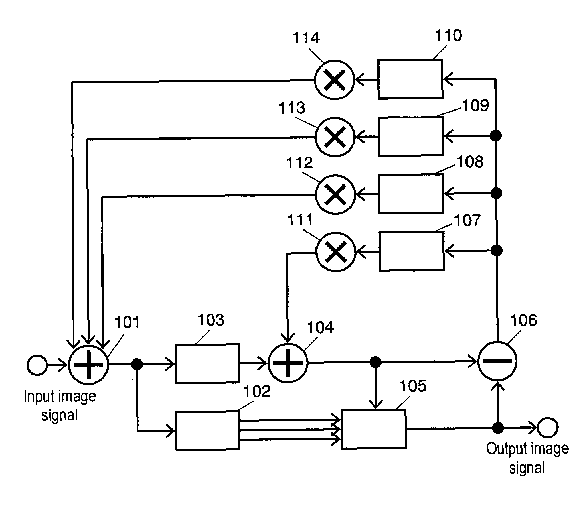
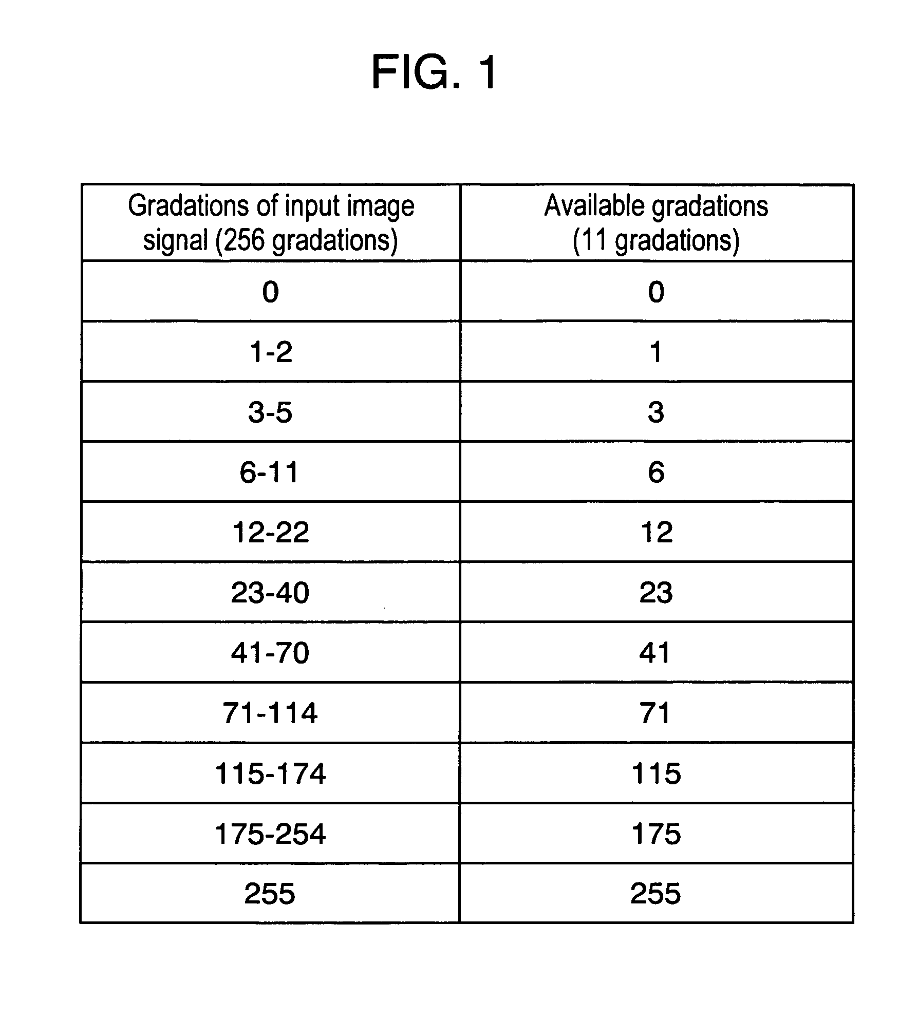
[0022]An image signal processing device in accordance with an exemplary embodiment of the present invention will be described hereinafter with reference to the following drawings. FIG. 1 is a diagram showing correspondence between available gradations and gradations of an input image signal in the exemplary embodiment of the present invention. In the present embodiment, the available gradations are 0, 1, 3, 6, 12, 23, 41, 71, 115, 175, and 255, and the 256 gradations of 0 to 255 are displayed using these 11 gradations. It is assumed that one frame is formed of 852×480 pixels and one-data period is about 41 ns. The present invention is not limited to these values.

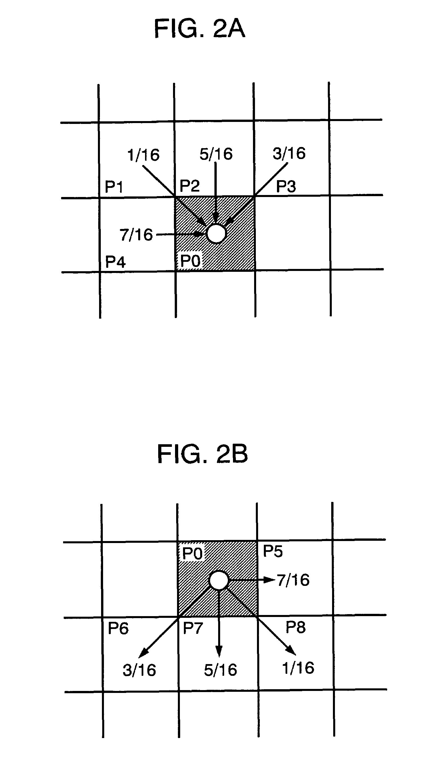
[0023]A concept of an image signal processing method of the present invention is first described. FIGS. 2A and 2B are diagrams showing a basic concept of the error diffusion processing. As shown in FIG. 2A, attention is focused on one pixel P0, and a corresponding image signal is assumed to be input. Display errors of pixels...


PUM


Abstract

A first adding circuit sums an input image signal of a target pixel and a value that is derived by multiplying respective display errors of three pixels, which are before the target pixel by one line, by weighting factors. A gradation candidate converter converts the gradation of the summed image signal to a plurality of available gradation candidates that are convertible when an error of the immediate left pixel is added. A delaying circuit delays the summed image signal. A second adding circuit sums the delayed image signal and a value that is derived by multiplying the error generated in the immediate left pixel by a weighting factor. A gradation selector selects a gradation closest to the gradation of the image signal to which the error is added from a plurality of gradation candidates, and outputs it as an image signal of the target pixel. A differencing circuit determines a display error of the target pixel.

Description

TECHNICAL FIELD[0001]The present invention relates to an image signal processing device and image signal processing method for eliminating image quality reduction due to shortage of gradation, in a display device for displaying a digital input image signal with multiple gradations.BACKGROUND ART[0002]When a display device where the number of displayable gradations is small performs multiple gradation display, smooth variation of brightness cannot be displayed. The brightness varies in steps, a contour-like pattern appears, and the image quality is reduced.[0003]For example, a display device such as a plasma display panel (PDP) or a digital mirror device (DMD) displays multiple gradations by dividing one field to a plurality of subfields having different luminance weights and combining light emission and non-emission in each subfield. It is known that specific noise, known as a motion picture pseudo-outline, occurs in a motion picture part in this display device. For preventing the o...

Claims


Application Information

Patent Timeline
Patent Type & Authority Patents(United States)
IPC IPC(8): G09G5/10G09G3/28G09G5/02G09G3/20G09G3/34H04N1/40H04N1/405H04N1/41
CPCG09G3/2066G09G3/28G09G3/34H04N1/40087H04N1/4052
Inventor YAMADA, KAZUHIRO
Owner PANASONIC CORP
Why Eureka
Try Eureka