Impedance circuit, power supply device
a technology of impedance circuit and power supply device, which is applied in the direction of logic circuit using specific components, logic circuits using semiconductor devices, pulse techniques, etc., can solve the problems of increasing the internal resistance of the battery, deteriorating performance, and the inability of sensing pair wires to always be connected near the load, so as to achieve the effect of negative impedance with eas
- Summary
- Abstract
- Description
- Claims
- Application Information
AI Technical Summary
Benefits of technology
Problems solved by technology
Method used
Image
Examples
first embodiment
[0036]In this embodiment, an impedance circuit using a current inverter circuit will be described.
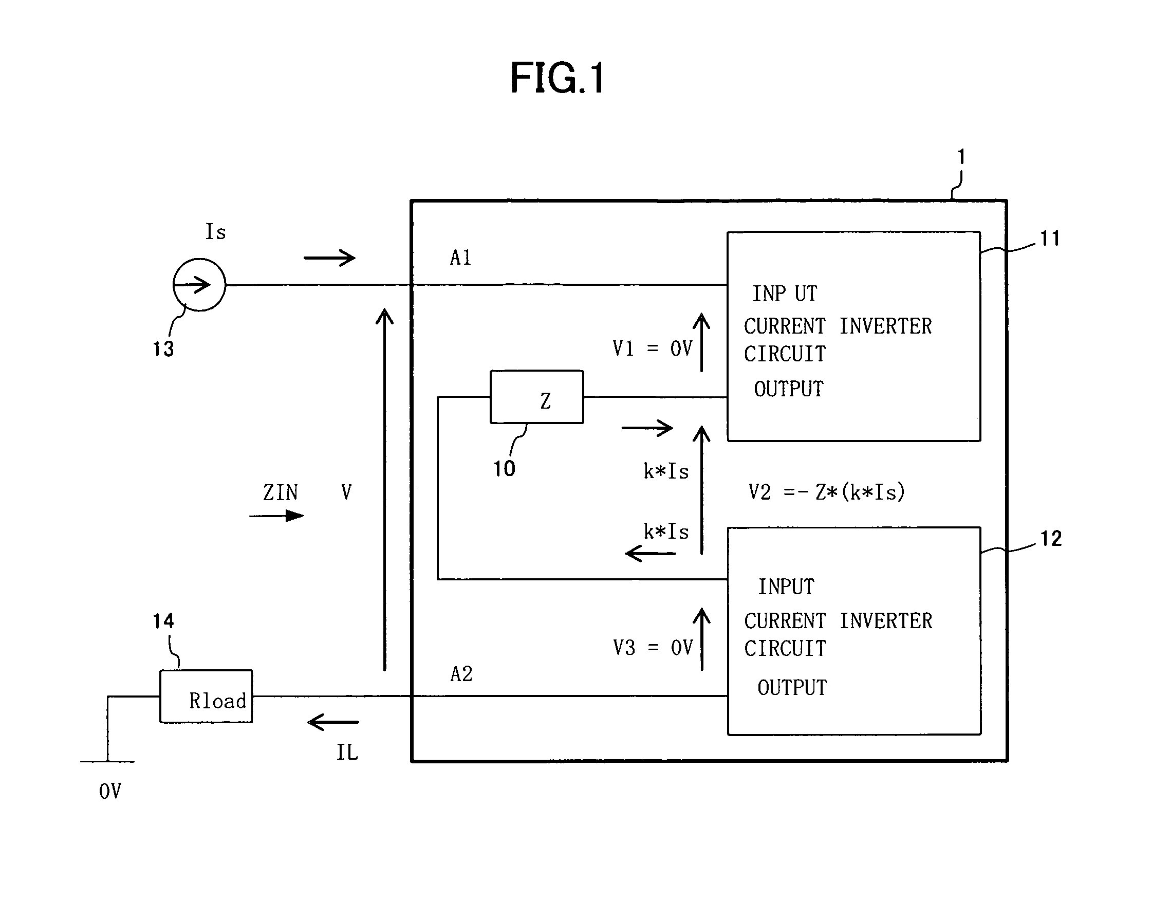
[0037]The structure of an impedance circuit according to the present invention will now be described first. FIG. 1 is a circuit diagram showing an example of the structure of the impedance circuit according to the present invention. This impedance circuit 1 has a passive circuit 10, and current inverter circuits 11 and 12. An input terminal of the impedance circuit 1 is denoted as A1, and an output terminal thereof is denoted as A2.
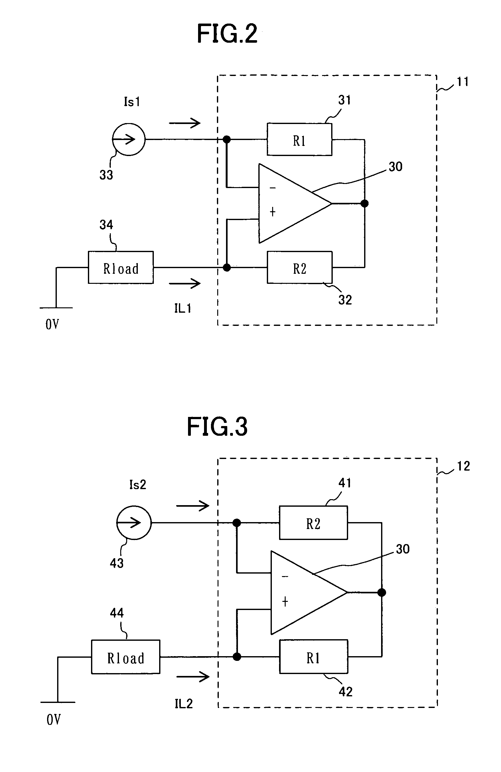
[0038]The input terminal of the current inverter circuit 11 is connected to an external current source 13 through A1. An output terminal of the current inverter circuit 11 is connected to an input terminal of the passive circuit 10. An input terminal of the current inverter circuit 12 is connected to an output terminal of the passive circuit 10. An output terminal of the current inverter circuit 12 is connected to an external load 14 through A2. The current i...
second embodiment
[0055]In the present embodiment, an impedance circuit using another current inverter circuit will be described.
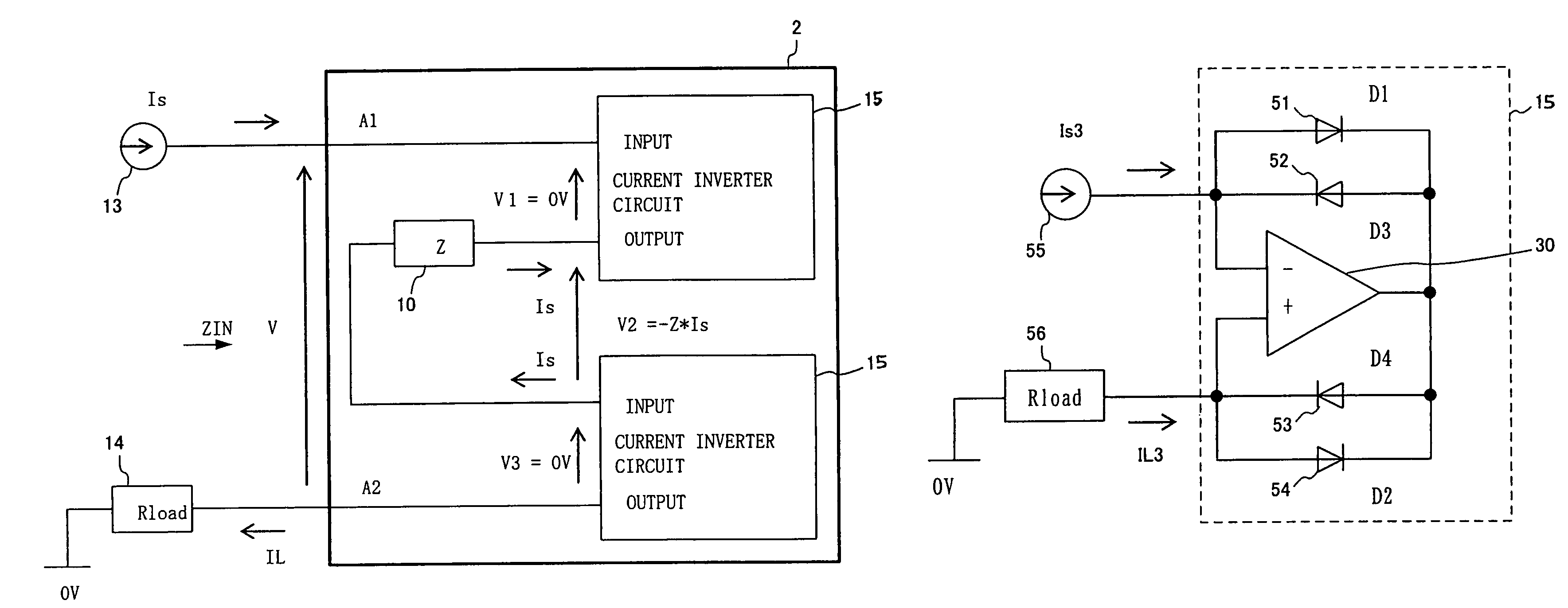
[0056]FIG. 4 is a circuit diagram showing another example of the structure of the impedance circuit according to the present invention. In FIG. 4, the same reference symbols as those of FIG. 1 denote identical or equivalent components to those shown in FIG. 1. Descriptions thereof will be omitted herefrom. Compared with FIG. 1, an impedance circuit 2 in place of the impedance circuit 1 is included in FIG. 3. Compared with the impedance circuit 1, the impedance circuit 2 has two current inverter circuits 15 in place of the current inverter circuits 11 and 12.
[0057]The current inverter circuits 15 will be described next.
[0058]FIG. 5 is a circuit diagram showing a third example of the structure of the current inverter circuit according to the present invention. In FIG. 5, the same reference symbols as those of FIG. 2 denote identical or equivalent components to those shown in ...
third embodiment
[0062]In the present embodiment, a power supply device using an impedance circuit described above will be described.
[0063]FIG. 6 is a circuit diagram showing an example of the structure of a power supply device using the impedance circuit according to the present invention. In FIG. 6, the same reference symbols as those of FIG. 8 denote identical or equivalent components to those shown in FIG. 8. Descriptions thereof will be omitted herefrom. Compared with FIG. 8, FIG. 6 shows a resistor 113 in place of the resistor 103 as well as a resistor 114 in place of the resistor 104.
[0064]In this example, the resistor 114 is a resistance which a current path between a power supply section 101 and a load 102 has. The resistance value of the resistor 114 is expressed by RL1+RL2. At this time, an impedance circuit as described above is adopted as the resistor 113. The resistance value of the impedance circuit is set to a negative resistance −RL1−RL2. In this way, a voltage drop caused between t...
PUM
 Abstract
Description
Claims
Application Information
 - R&D
- Intellectual Property
- Life Sciences
- Materials
- Tech Scout
- Unparalleled Data Quality
- Higher Quality Content
- 60% Fewer Hallucinations
Browse by: Latest US Patents, China's latest patents, Technical Efficacy Thesaurus, Application Domain, Technology Topic, Popular Technical Reports.
© 2025 PatSnap. All rights reserved.Legal|Privacy policy|Modern Slavery Act Transparency Statement|Sitemap|About US| Contact US: help@patsnap.com


