Image display apparatus provided with an ion pump assembly arranged within an external container
a technology of ion pump and display apparatus, which is applied in the direction of tubes with screens, discharge tubes with luminescent screens, vacuum obtaining/maintenance, etc., can solve the problems of affecting the operation of the apparatus, and damaging the electron source, so as to achieve small changes in the properties of electron sources, high display quality, and high reliability
- Summary
- Abstract
- Description
- Claims
- Application Information
AI Technical Summary
Benefits of technology
Problems solved by technology
Method used
Image
Examples
embodiment 1
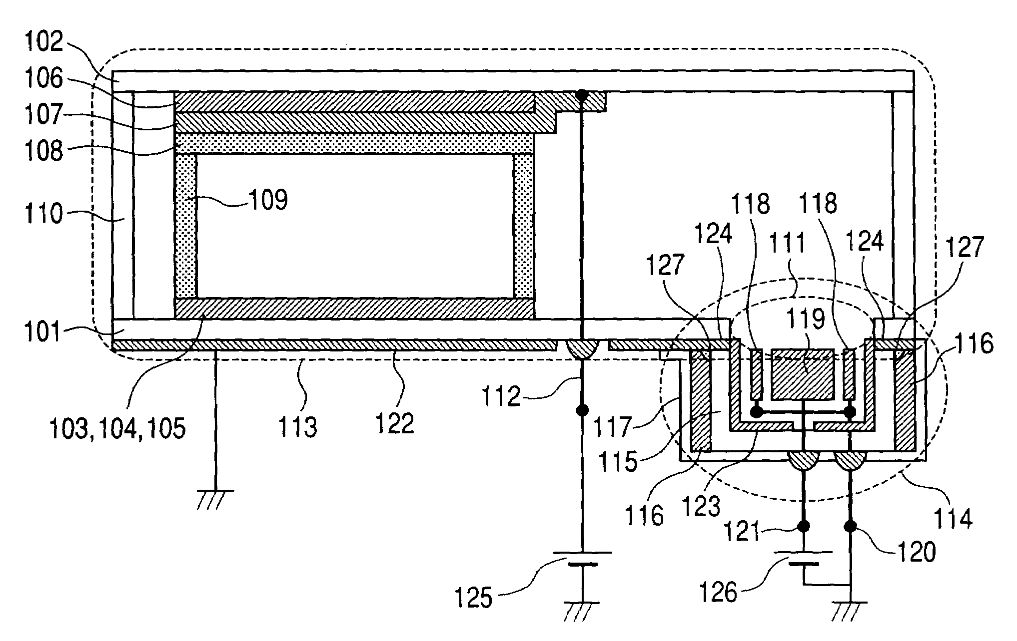
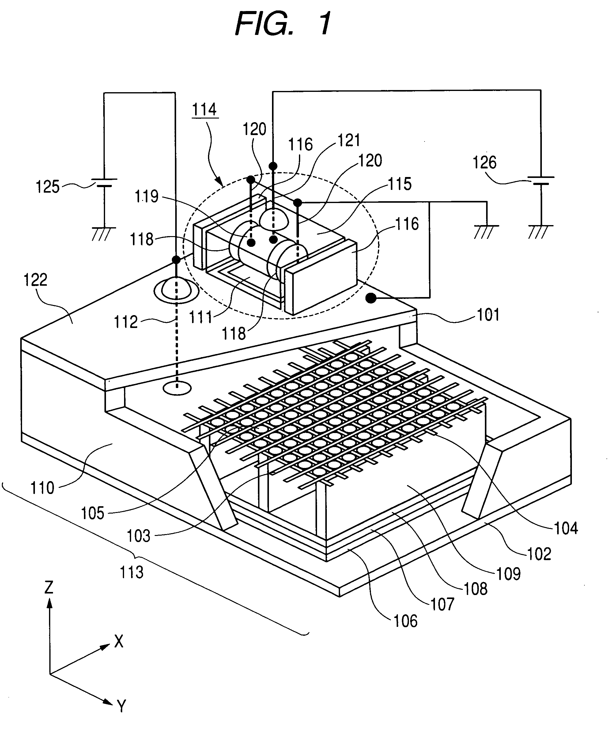
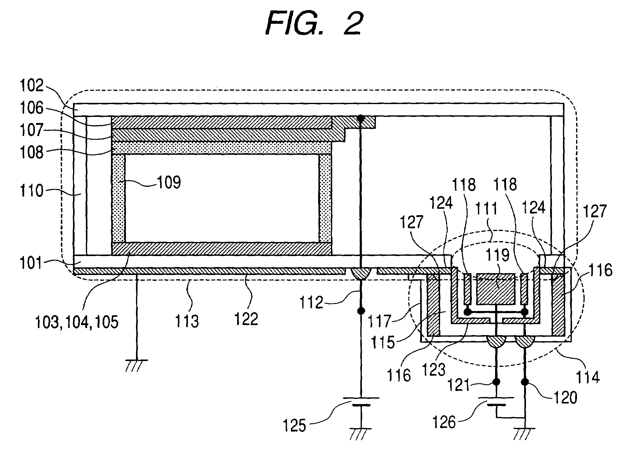
[0064]In this embodiment, an image display apparatus having a structure shown in FIG. 4, that is, an image display apparatus having an electroconductive film formed on the external surface of a rear plate was produced. The image display apparatus was provided with an electron source 105 having multiple (768 rows×3,840 columns) surface conduction electron-emitting devices wired in a simple matrix fashion on a substrate. Hereinafter, a method of producing the image display apparatus of this embodiment will be described.
[0065]Step-x1 (Production of Glass Substrate Attached with Electroconductive Film)
[0066]A glass substrate 301 of PD-200 (manufactured by Asahi Glass Co., Ltd.) having a thickness of 2.8 mm was washed with a detergent, pure water, and an organic solvent, and an ITO film having a thickness of 0.3 μm was formed on one surface of the substrate by means of ordinary sputtering. Then, the ITO film was patterned by means of ordinary photolithography to remove a high voltage ter...
embodiment 2
[0104]In this embodiment, an image display apparatus having a structure shown in FIG. 9, that is, an image display apparatus having an electroconductive film formed on the external surface of a rear plate and an electroconductive film formed on the internal surface of an ion pump container was produced.
[0105]Steps-x2 and a2 To g2
[0106]Steps similar to the steps-x1 and a1 to g1 described in Embodiment 1 were repeated.
[0107]Step-y2 (Assembly and Attachment of Ion Pump)
[0108]First, a glass container 115 for an ion pump perforated with holes for ion pump anode and cathode terminals was prepared. The holes may be formed by melting, or may be formed mechanically by means of a microprocessing grinding attachment. After the glass container had been washed with an organic solvent, a photoresist was applied to a predetermined position inside the glass container by means of a plate, and the whole was baked at 90° C. for 10 minutes to form a pattern for lift-off. In this state, a solution prepa...
embodiment 3
[0113]In this embodiment, an image display apparatus having a structure shown in FIG. 10, that is, an image display apparatus having an electroconductive film formed on the external surface of a rear plate and an electroconductive film formed on the internal surface of an ion pump container, the electroconductive film on the external surface of the rear plate being removed at a portion to be connected to an ion pump, was produced.
[0114]Step-x3 (Production of Glass Substrate Attached with Electroconductive Film)
[0115]A glass substrate 301 of PD-200 (manufactured by Asahi Glass Co., Ltd.) having a thickness of 2.8 mm was washed with a detergent, pure water, and an organic solvent, and an ITO film having a thickness of 0.3 μm was formed on one surface of the substrate by means of ordinary sputtering. Then, the ITO film was patterned by means of ordinary photolithography to remove a high voltage terminal portion and a portion to be bonded to the ion pump container in a subsequent step.
[...
PUM
 Abstract
Description
Claims
Application Information
 - R&D
- Intellectual Property
- Life Sciences
- Materials
- Tech Scout
- Unparalleled Data Quality
- Higher Quality Content
- 60% Fewer Hallucinations
Browse by: Latest US Patents, China's latest patents, Technical Efficacy Thesaurus, Application Domain, Technology Topic, Popular Technical Reports.
© 2025 PatSnap. All rights reserved.Legal|Privacy policy|Modern Slavery Act Transparency Statement|Sitemap|About US| Contact US: help@patsnap.com


