
Test method for nonvolatile memory

a non-volatile memory and test method technology, applied in the direction of digital storage, static storage, instruments, etc., can solve the problems of inability to perform high-speed rewriting operations, test apparatus cannot make a correct determination, and cannot perform writing operations, etc., to achieve the effect of simplifying the test program

Inactive Publication Date: 2007-11-06
LAPIS SEMICON CO LTD
View PDF5 Cites 15 Cited by
  • Summary
  • Abstract
  • Description
  • Claims
  • Application Information

AI Technical Summary

Benefits of technology

The present invention provides improved methods for testing nonvolatile memories. These methods simplify the test program, allow for writing and reading tests as a series of tests, and are compatible with multi-bit and pin-multiplex techniques. The methods involve connecting the test apparatus to the nonvolatile memory using n input and output terminals, and monitoring the output timing of the completion signal from the nonvolatile memory. The methods also allow for a simple test program and make it possible for the writing and reading tests to be a series of tests. The test apparatus can have different configurations depending on the number of data terminals and the speed of the clock signal. The technical effects of the invention include simplifying the testing process, improving efficiency, and ensuring compatibility with various memory configurations.

Problems solved by technology

Due to property inherent in the memory device, it is impossible to perform a high speed rewriting operation that is realized by a memory with a flip-flop.
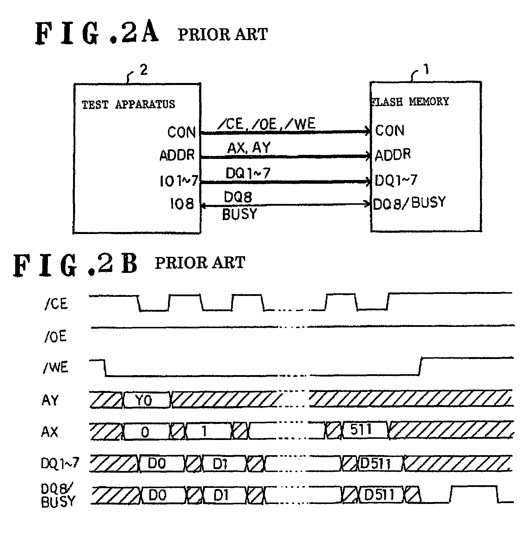
(1) The input and output terminal IO8 of the test apparatus 2 needs an alternate switching operation between outputting of the writing data and inputting of the busy signal even during the writing test. Further, the writing test is immediately followed by a reading test in this test method, but a strobe condition of the reading test is different from that of the writing test. Accordingly, a test program for the test apparatus 2 becomes complicated and a programming and a debugging step therefor become time consuming, thereby prolonging a period for a development of the devices such as the flash memory 1.
(2) In a test apparatus having an ALPG (Algorithmic Pattern Generator), data with a specific pattern is output from the input and output terminal IOi and is written to a memory, and then the data which is read from the memory is compared with the specific pattern. When such test apparatus is used for the test of the flash memory 1 in a manner shown in FIG. 2A, the test apparatus can not make a correct determination because the input and output terminals IO8 receives the data DQ8 and the busy signal BUSY in a time-division manner. Accordingly, it is impossible to perform a writing operation and a reading operation consecutively in a single test.
(3) There is a test apparatus having a plurality of test circuits each compatible with a certain number of bits, e.g., 8 bits, such that the same test can be simultaneously performed for a plurality of flash memories. When such test apparatus is used to test a flash memory with 16 bits, two test circuits are necessary for a single flash memory, but the flash memory has only one multifunction terminal DQ16 / BUSY. Consequently, use of merely two sets of the test circuits each having a configuration shown in FIG. 2A can not test the 16-bit flash memory.
(4) A test apparatus has a certain maximum operation frequency, and thus it is impossible to perform a high speed performance test with a frequency higher than the maximum operation frequency by means of a conventional measurement method. On the other hand, there is a test apparatus capable of performing a technique called pin-multiplex, in which two input and output terminals IOi is made to be a pair, and the clocks thereof are respectively distributed to a first half clock and a last half clock within a cycle so that a clock with pseudo doubled frequency is output. Use of such technique, however, causes such problems that the same data are always issued from the paired input and output terminals IOi, and the same decision procedures for expected values are established in the reading test. Accordingly, since only one input and output terminal IOi is not enough to monitor the busy signal BUSY, no flash memory can be tested by merely using the pin-multiplex in a manner shown in FIG. 2A.

Method used


Image

  • Test method for nonvolatile memory
  • Test method for nonvolatile memory
  • Test method for nonvolatile memory

Examples


first embodiment

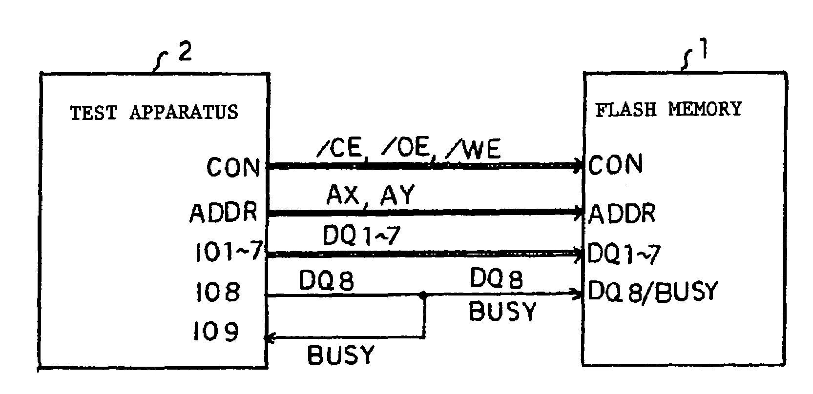
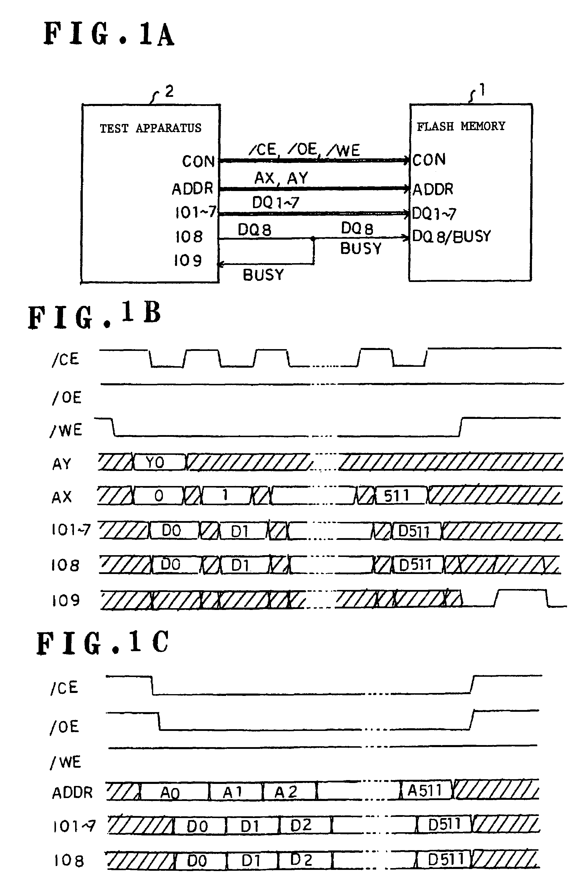
[0040]Referring to FIGS. 1A to 1C, there are shown a test method for a flash memory according to a first embodiment of the present invention. Specifically, FIG. 1A shows a block diagram of the test method, FIG. 1B shows a signal waveform chart during a writing test, and FIG. 1C shows a signal waveform chart during a reading test.

[0041]As shown in FIG. 1A, a flash memory 1 to be tested includes a control terminal section CON, an address terminal section ADDR, bidirectional data terminals DQ1-DQ7, and a multifunctional terminal DQ8 / BUSY. The control terminal section CON has a plurality of terminals for receiving control signals such as a chip selection signal / CE, an output control signal / OE, and a writing control signal / WE. The address terminal section ADDR has a plurality of terminals. The number of the terminals corresponds to the number of bits of address signals, which respectively designate addresses in a memory area such that whole memory area is covered by the address signal...

second embodiment

[0067]FIGS. 3A and 3B illustrate a test method for a flash memory according to a second embodiment of the present invention. Specifically, FIG. 3A is a diagram illustrating the test method, while FIG. 3B is a signal waveform chart during a writing test.

[0068]This test method employs a test apparatus 2A having two test circuits each compatible with 8 bits so that this method allows simultaneous testing of two memories each having 8 bit-width. Accordingly, this method allows testing of a flash memory 1A with 16 bits data width.

[0069]As shown in FIG. 3A, a control terminal section CON and an address terminal section ADDR of the flash memory 1A to be tested are respectively connected to those of the test apparatus 2A.

[0070]Further, data terminals DQ1-DQ7 and a data terminal DQ8 of the flash memory 1A are respectively connected to input and output terminals IO1-IO7 and an input terminal IO8 of a test circuit T1 of the test apparatus 2A. Data terminals DQ9-DQ15 of the flush memory 1A are ...

third embodiment

[0079]FIGS. 4A and 4B illustrate a test method for a flash memory according to a third embodiment of the present invention. Specifically, FIG. 4A is a diagram illustrating the test method, while FIG. 4B is a signal waveform chart during a writing test.

[0080]This test method employs a pin multiplex approach, in which reading and writing tests for the flash memory 1 are carried out at a rate equal to or faster than the maximum operating frequency available in a test operation of the test apparatus 2B.

[0081]The test apparatus 2B has two ALPGs, i.e., a main ALPG and a secondary ALPG. In a first half in each cycle, a test signal is output from the main ALGP, while in a last half of the cycle the test signal is output from the secondary ALPG.

[0082]As shown in FIG. 4A, a main control terminal CONM and a secondary control terminal CONS of the test apparatus 2B are connected to a control terminal CON of the flash memory 1 via a logical sum gate (hereinafter referred to as ‘OR’) 3a. A main ad...


PUM


Abstract

A control terminal section CON and an address terminal section ADDR of a test apparatus are respectively connected to those of a flash memory. A first to an (n−1) -th input and output terminal of the test apparatus are connected to data terminals of the flash memory. Further, an n-th and an (n+1)-th input and output terminal of the test apparatus are connected to a multifunctional terminal of the flash memory. The (n+1)-th input and output terminal is established as a dedicated terminal to receive data supplied to the test apparatus. The first to the n-th input and output terminal of the test apparatus are used to output the writing data to the flash memory, while the (n+1)-th input and output terminal is used to detect the completion signal output from the flash memory.

Description

BACKGROUND OF THE INVENTION[0001]1. Field of the Invention[0002]The invention relates to a method for testing a nonvolatile memory such as a flash memory which outputs a completion signal upon completion of a writing operation or an erasing operation in the memory.[0003]2. Description of the Related Art[0004]A flash memory employs a field-effect transistor with a floating gate as a memory device to write and erase data by accumulating an electrical charge to the floating gate and by discharging the accumulated electrical charge from the floating gate. Since the electrical charge in the insulated floating gate is retained even after a power source is disconnected, the flash memory is referred to as a nonvolatile memory. One example of the flash memory is disclosed in Japanese Patent Kokai No. 2000-40389.[0005]The flash memory includes a control circuit which performs page-by-page writing of the data, e.g. 512 bytes in one page, and block-by-block erasing of the data, e.g. 32 pages in...

Claims


Application Information

Patent Timeline
Patent Type & Authority Patents(United States)
IPC IPC(8): G11C29/00
CPCG11C29/56012G11C29/48G11C16/04G11C29/022
Inventor HOBARA, TETSUYA
Owner LAPIS SEMICON CO LTD
Learn More