Power-on reset circuit

a power-on reset and circuit technology, applied in electronic switching, pulse automatic control, pulse technique, etc., can solve the problems of unnecessary power consumption, more power consumption in the charging/discharging process, etc., to prolong the turn-on time of the power-on reset circuit, reduce the effect of resistan

Active Publication Date: 2007-09-25
XIAMEN XM PLUS TECH LTD
View PDF8 Cites 3 Cited by
  • Summary
  • Abstract
  • Description
  • Claims
  • Application Information

AI Technical Summary

Benefits of technology

[0012]Accordingly, the present invention is directed to a power-on reset circuit to reduce the capacitance and capacitor area of the resistance-capacitance (RC) time delay, and to reduce current consumption. In addition, the capacitor charging direction in determining the RC time delay is fixed, so the system operation is stable and noises are reduced.
[0021]The present invention uses the clock signal and the reset of the signal to effectively control the switch time of resistors or transistors so as to extend the turn-on time of the power-on reset circuit. The present invention adjusts amplitudes and period time of the clock signals. The control of the amplitudes of the clock signals is related to the turn-on voltage of the transistor. The control of the period time of the clock signals is performed by shaping waveforms of the amplitude-restricted clock signal with about, for example, 50% duty cycle into the control signals which can turn on the route with the transistor in a shorter time, such as smaller than 50% duty cycle. Accordingly, the RC time delay formed by a small resistance and a small capacitor area can be achieved. Due to elimination of the current leakage route in the operation, the leakage consumption can be reduced. Moreover, the charging direction for determining the time constant is fixed, so no reverse signals will enter into the circuit from the ground terminal. Noises passing through the substrate can be prevented.

Problems solved by technology

Moreover, the resistor 111 forms a leakage route that consumes unnecessary power.
Moreover, the charging / discharging process will consume more power.

Method used


Image

  • Power-on reset circuit
  • Power-on reset circuit
  • Power-on reset circuit

Examples


Embodiment Construction

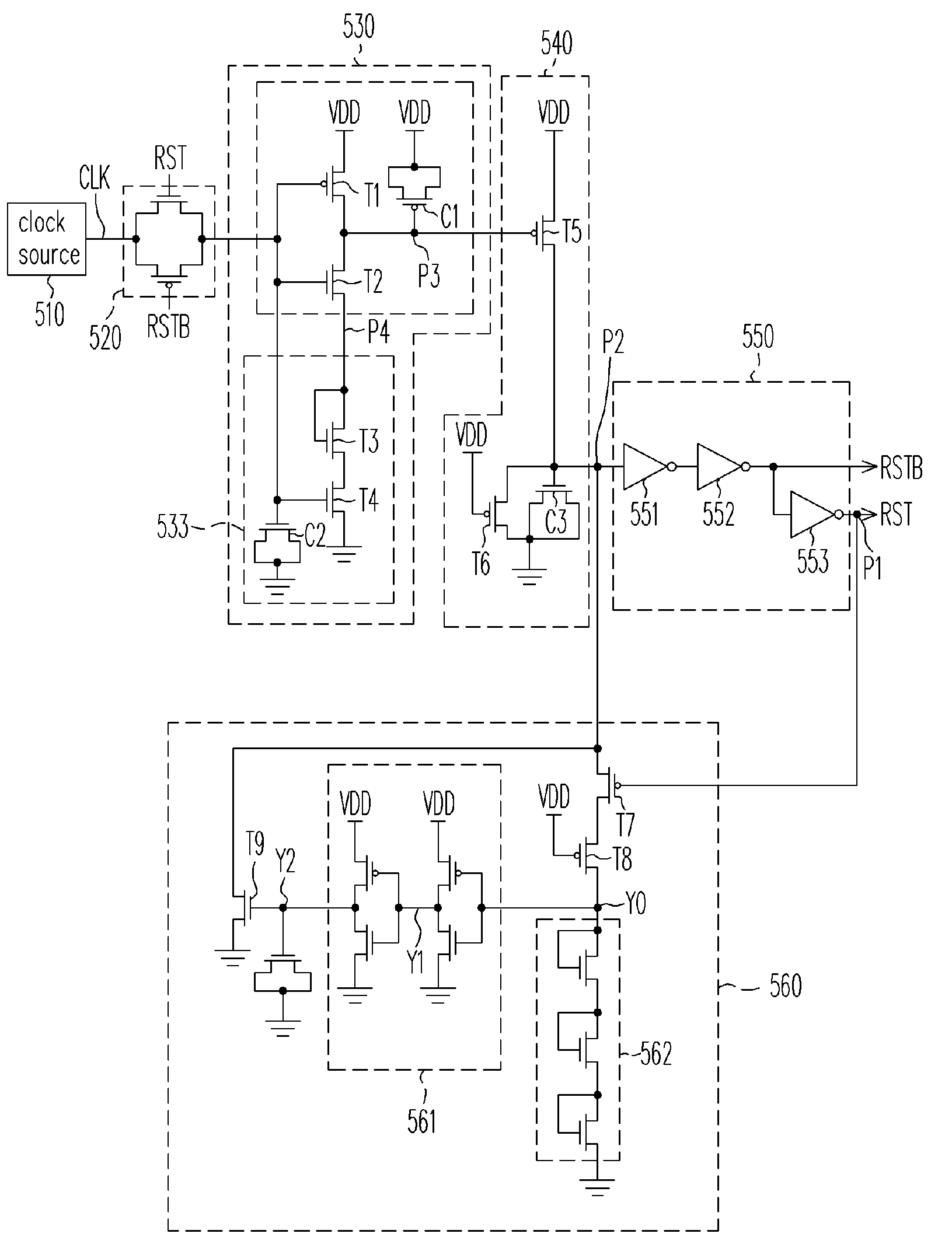
[0034]FIG. 3A is a power-on reset circuit according to an embodiment of the present invention. Referring to FIG. 3A, the clock source 310 generates a clock signal CLK. The control switch 320 comprises a first connection terminal, a second connection terminal, and a control terminal. The control switch 320 determines whether to transmit the clock signal CLK received by the first connection terminal to the second connection terminal and to output the clock signal CLK to the adjusting circuit 330 according to the reset signal RST. In this embodiment, it is assumed that the initial condition of the control switch 320 is turn-on.

[0035]The adjusting circuit 330 receives and adjusts the clock signal CLK to output the control signal 331. In this embodiment, the adjustment of the signal comprises restricting the amplitude and the time of the clock signal CLK. Wherein, the restriction of the amplitude is related to the turn-on voltage for controlling charge / discharge. For example, the clamp c...


PUM


Abstract

A power-on reset circuit is provided. The power-on reset circuit includes an adjusting circuit, a charging / discharging unit and an output circuit. The adjusting circuit receives and adjusts a clock signal so as to output a control signal, wherein a minimum level of the control signal is clamped to be higher than a pre-defined level. The charging / discharging unit having a capacitor apparatus receives the control signal, determines whether to charge / discharge the capacitor apparatus based on the control signal, and outputs a storage voltage of the capacitor apparatus. The output circuit receives the storage voltage and outputs the reset signal. Wherein, the adjusting circuit determines the charging / discharging duty cycle of the charging / discharging unit by adjusting the waveform and the minimum level of the control signal. The output circuit enables / disables the reset signal according to whether the storage voltage reaches the threshold voltage of the output circuit.

Description

CROSS-REFERENCE TO RELATED APPLICATION[0001]This application claims the priority benefit of Taiwan application serial no. 93136261, filed on Nov. 25, 2004. All disclosure of the Taiwan application is incorporated herein by reference.BACKGROUND OF THE INVENTION[0002]1. Field of the Invention[0003]The present invention relates to a circuit for generating a reset signal, and more particularly to a power-on reset circuit.[0004]2. Description of the Related Art[0005]For design of electronic circuits, a reset mechanism is normally added in these circuits so that these circuits can come back to an initial condition when necessary. Particularly at the beginning these electronic circuits being turned on, devices, such as registers, in these circuits are not stable, it is essential to reset the circuit to let these devices of these circuits be back to the initial condition.[0006]Accordingly, a circuit is required to generate a reset signal at the beginning of the turn on of the circuit so tha...

Claims


Application Information

Patent Timeline
Patent Type & Authority Patents(United States)
IPC IPC(8): H03L7/00H03K3/02H03K17/22H03K17/30
CPCH03K17/223H03K17/302
Inventor HSU, PO-CHIN
Owner XIAMEN XM PLUS TECH LTD
Why Eureka
Try Eureka