Integrated approach for design, simulation and verification of monolithic, silicon-based opto-electronic circuits

a silicon-based opto-electronic circuit and integrated circuit technology, applied in the direction of electric/magnetic computing, instruments, analogue processes for specific applications, etc., can solve the problems of spice simulation extremely slow, pre-defined set of cells of a standard cell library may not provide the desired speed, size or power consumption,

Active Publication Date: 2007-09-11
CISCO TECH INC
View PDF28 Cites 20 Cited by
  • Summary
  • Abstract
  • Description
  • Claims
  • Application Information

AI Technical Summary

Problems solved by technology

At times, the pre-defined set of cells of a standard cell library may not provide a desired function, or may not provide the speed, size or power consumption desired.
However, SPICE simulation is extremely slow when compared to simulation employing an HDL netlist model.
When designs include both standard cell and custom logic sections, a problem arises when attempting to simulate the entire design.
A behavioral model, such as may be written in the C programming language, may be employed for function simulation, but such models do not allow for timing analysis.
As such, today's optics industry lacks a common technology platform to integrate different components (building blocks) to make a subsystem.
As a result, the current optical industry at large has a highly “un-integrated” approach for designing, simulating and verifying the mostly discrete optical components and optical systems.
The few existing design, simulation and verification tools for optical elements tend to be overly specific to a particular type of optical device, or a system of optical components.
Indeed, these tools have generally been developed for III-V based optical devices, not the silicon components used in the inventive integrated arrangement.
Optical modeling, as mentioned above, has heretofore been limited to use with traditional III-V-based optical devices.

Method used


Image

  • Integrated approach for design, simulation and verification of monolithic, silicon-based opto-electronic circuits
  • Integrated approach for design, simulation and verification of monolithic, silicon-based opto-electronic circuits
  • Integrated approach for design, simulation and verification of monolithic, silicon-based opto-electronic circuits

Examples


Embodiment Construction

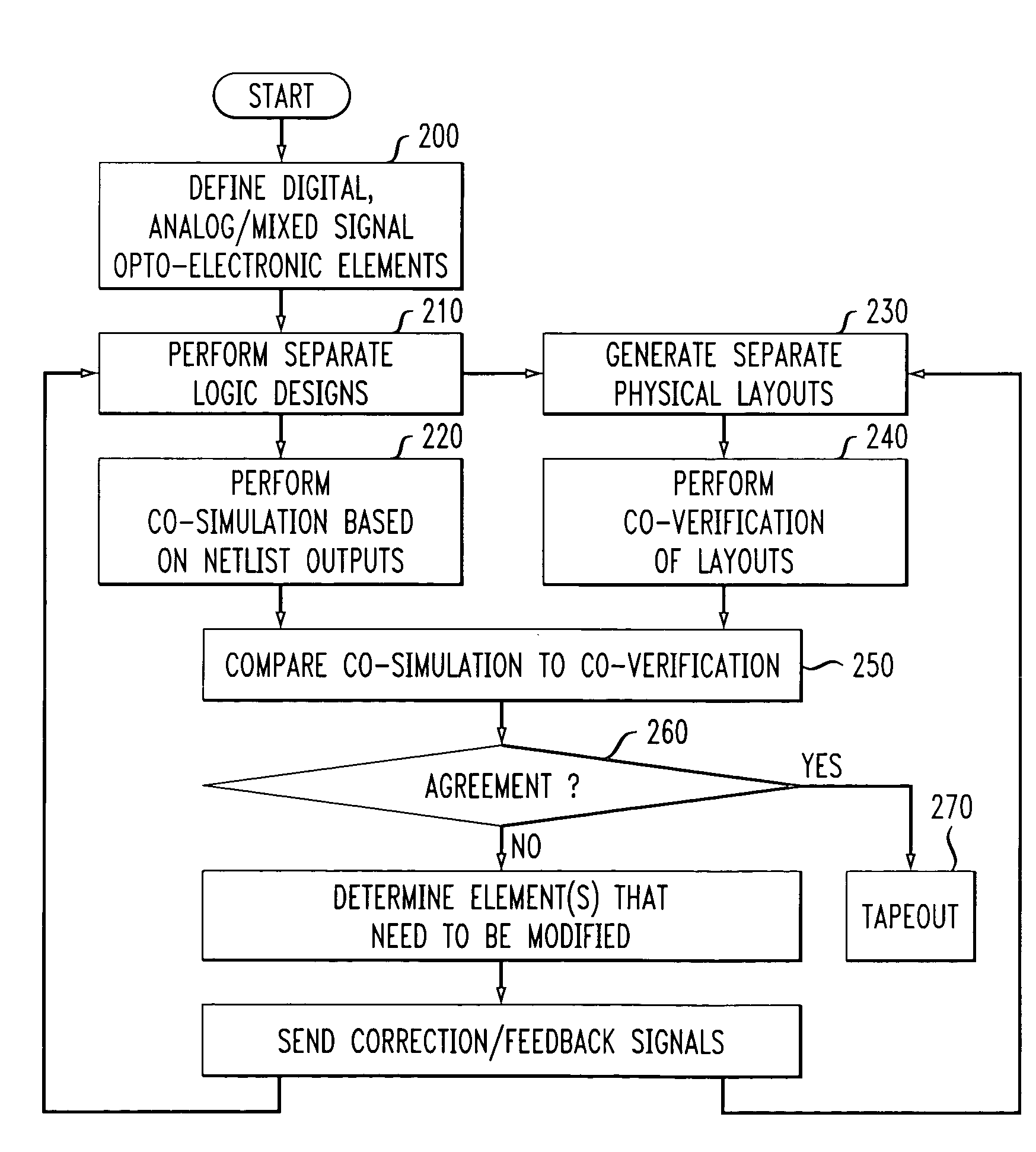
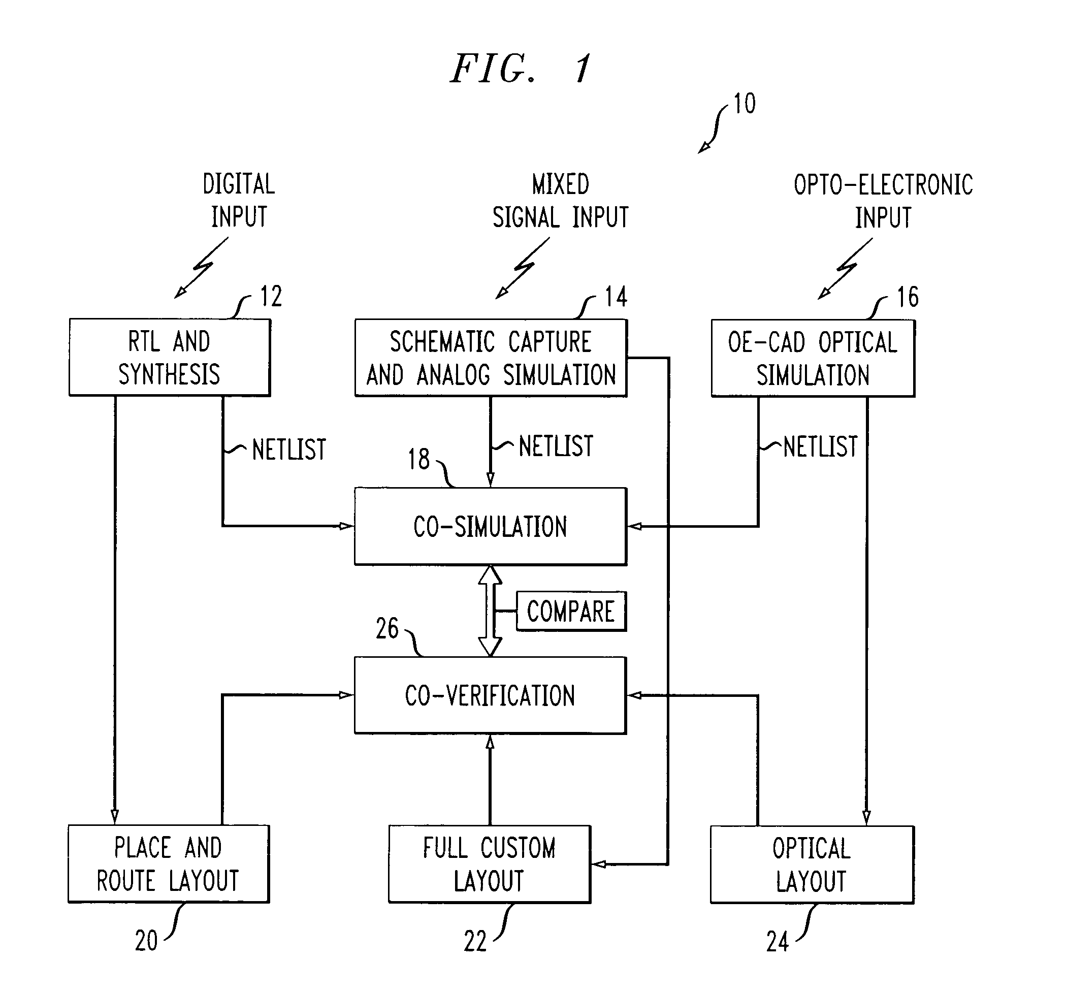
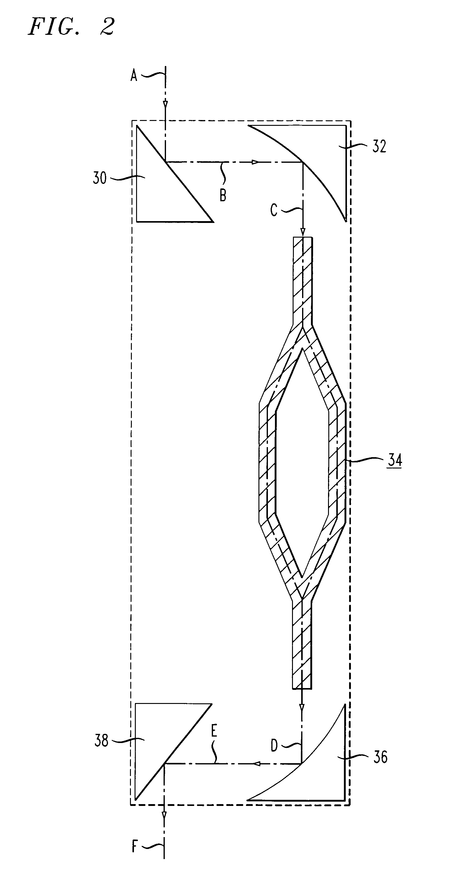
[0022]In its most general sense, the present invention can be viewed as performing separate top-level behavioral logic designs for the three different types of elements included within the final, silicon-based monolithic structure. The three different types of elements, as mentioned above, can be defined as: (1) digital electronic integrated circuit elements; (2) analog / mixed signal electronic integrated circuit elements; and (3) opto-electronic elements (including passive and active optical elements). Once the behavioral logic design is completed, the results are combined and co-simulated. A physical layout design is developed and verified for each different type of element in the circuit. The separate physical layouts are then co-verified, using a pre-defined set of test vectors, to measure the properties of the overall physical design. The annotated results (complete with definitions of parasitic capacitances and resistances, for example) is then re-simulated and compared with th...


PUM


Abstract

Computer-aided design (CAD) tools are used to perform the integrated design, verification and layout of electrical and optical components in a monolithic, silicon-based electro-optic chip. Separate top-level behavioral logic designs are prepared for the three different types of elements included within the final, silicon-based monolithic structure: (1) digital electronic integrated circuit elements; (2) analog / mixed signal electronic integrated circuit elements; and (3) opto-electronic elements (including passive and active optical elements). Once the behavioral logic design is completed, the results are combined and co-simulated. A physical layout design is developed and verified for each different type of element in the circuit. The separate physical layouts are then co-verified, to assess the properties of the overall physical design. The results of the co-simulation are compared to the results of the co-verification, with alterations made in the logic design and / or the physical layout until the desired operating parameters are obtained. Once the desired results are generated, conventional wafer-level fabrication operations are then considered to provide a final product (“tape out”).

Description

CROSS-REFERENCE TO RELATED APPLICATIONS[0001]This application claims the benefit of Provisional Application No. 60 / 582,235, filed Jun. 23, 2004.TECHNICAL FIELD[0002]The present invention relates to the automated design, layout and verification of integrated circuits and, more particularly, to the co-simulation and co-verification of both the optical and electrical circuit arrangements present in a silicon-based opto-electronic circuits.BACKGROUND OF THE DISCLOSURE[0003]Today's integrated circuits consist of as many as a billion transistors, a large number of input / output pins, and provide extensive functionality. To support the design, simulation, verification, place-and-route, and layout of these integrated circuits at the system, chip and logic levels, the integrated circuit (IC) industry has developed highly robust, well-established and standardized computer-aided design (CAD) tools, particularly electronic CAD (E-CAD) and methodologies. The E-CAD tools support digital, analog or...

Claims


Application Information

Patent Timeline
Patent Type & Authority Patents(United States)
IPC IPC(8): G06F17/50G06F17/10G06G7/62
CPCG06F17/5036G06F17/5068G06F30/367G06F30/39
Inventor SHASTRI, KALPENDUPATHAK, SOHAMGOTHOSKAR, PRAKASHMOSINSKIS, PAULIUSDAMA, BIPIN
Owner CISCO TECH INC
Why Eureka
Try Eureka