
Device for recording laser trim progress and for detecting laser beam misalignment

a technology of laser beam and progress recording, applied in the field of electromechanical circuitry, can solve problems such as circuit under trim failure, component or substrate damage, and circuit under trim damag

Active Publication Date: 2007-08-21
TEXAS INSTR INC
View PDF5 Cites 1 Cited by
  • Summary
  • Abstract
  • Description
  • Claims
  • Application Information

AI Technical Summary

Problems solved by technology

During laser trim, damage to the circuit under trim can occur (1) when the laser beam is not accurately aligned to the target links or (2) when a circuit is re-trimmed after a prior laser trim attempt.
These undesired trim incidences can result in component or substrate damage.
These inappropriate laser blasts may cause the circuit under trim to fail during post trim testing or, far worse, cause the trimmed circuit to fail prematurely in its final operating environment.
Such circuit structures do not directly enhance the functionality of the device.
However, many devices that use laser trim may not have digital circuitry in them and memory cell approach cannot be used in such devices.
These additional probe pads consume thousands of square microns of valuable device area in most circuit fabrication processes.

Method used


Image

  • Device for recording laser trim progress and for detecting laser beam misalignment
  • Device for recording laser trim progress and for detecting laser beam misalignment
  • Device for recording laser trim progress and for detecting laser beam misalignment

Examples


example 1

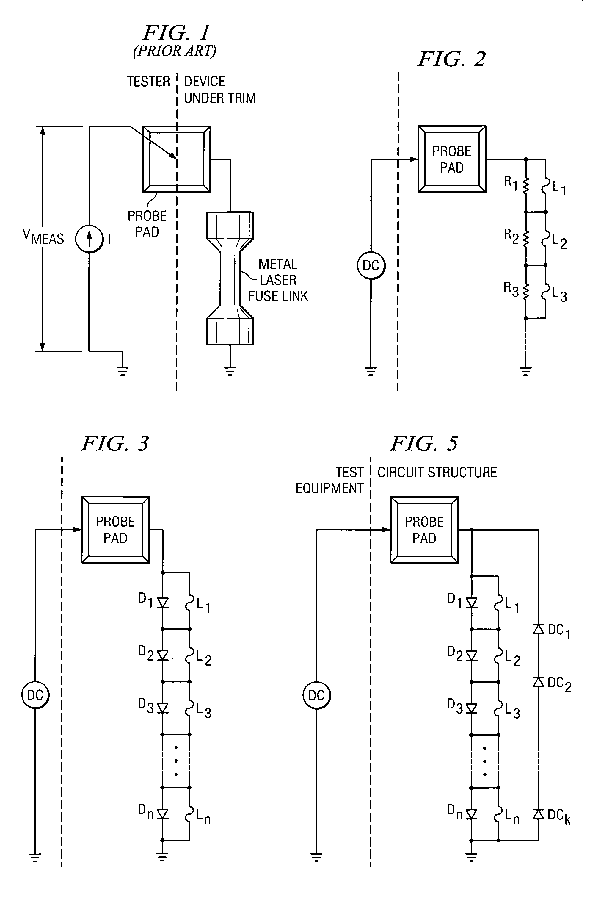
[0024]Trim network consists of 1K resistor with 20% process variation. This process variation will translate to 20% measurement variation. Thus, there are only 3 links per network.

example 2

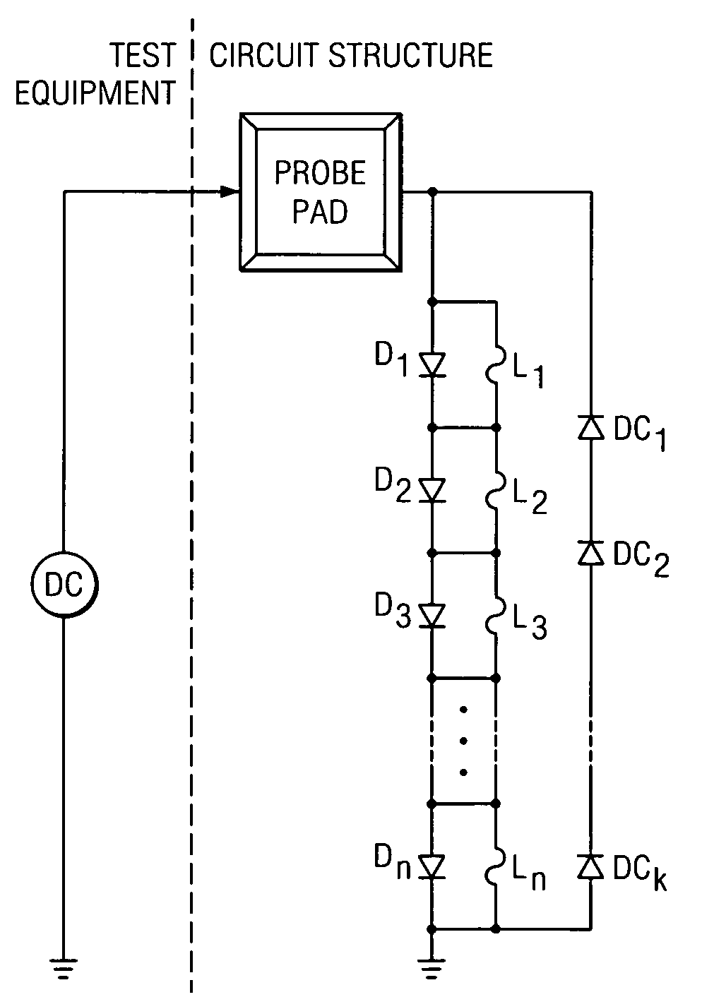
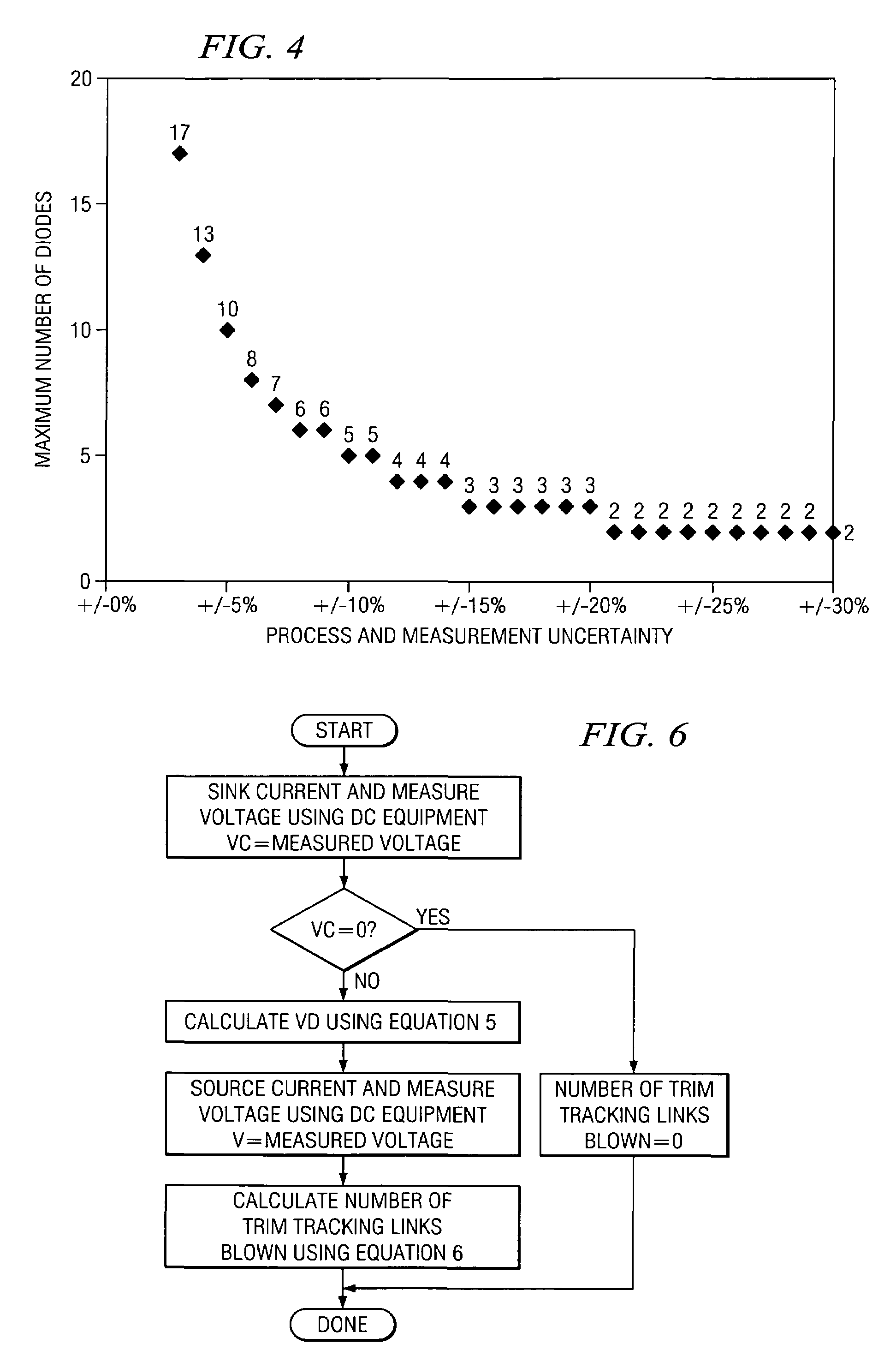
[0025]Trim network consists of diodes with 0.7V forward bias and 10% variation in diode drop. The 10% diode drop variation will translate to 10% measurement variation and thus there can be a maximum of 5 links per network. In general the non-ideal forward bias diode knee voltage may have a smaller process variation than the resistors and therefore, allow more diode link pairs and more incremental trim records.

[0026]From the description above and examples presented, it is clear that the key to increasing the number of trim tracking links per circuit structure is to reduce the measurement uncertainty. In semiconductor processing the absolute variation in the properties of an electrical component is typically very high. However, properties of components placed closely together are very well matched. If the electrical property of one of the components can be measured, that measurement can be used as m in the equations. Deviation of measurements on other components δm will be very small ...

example

[0033]Diodes in a technology have maximum forward bias drop Vdmax=0.8V, matching of 1%, and minimum break down voltage of Bvmin=4.0V. From Equation 2, the maximum number of trim tracking links nmax will be 50. The number of diodes in the calibration string will be

[0034]Kmin=50×(0.84)=10.

[0035]Test procedure that utilizes this circuit structure is shown in FIG. 6. The step by step procedure in determining the laser trim status is described below.

[0036]1. A DC current is sunk using the DC instrument. The calibration diode string gets forward biased. The voltage at the probe pad is measured using the voltmeter in the DC instrument and recorded as VC.

[0037]2. If VC is very close to zero that means there is a direct connection between probe pad and ground. Hence, the number of links blown will be equal to zero.

[0038]3. If VC is not close to zero, calculate the diode drop in the device using equation

[0039]Vd=VcK(Eq⁢⁢5)

[0040]4. Source a current using the DC equipment. This will forward bia...


PUM

PropertyMeasurementUnit
resistanceaaaaaaaaaa
voltageaaaaaaaaaa
electrically conductiveaaaaaaaaaa

Abstract

The device for detecting and tracking a status of a device under laser trim includes: a series connected string of trim tracking links; and a plurality of detecting devices wherein each detecting device is coupled in parallel with a corresponding trim tracking link. This device allows detection of laser beam to work surface misalignment and the termination of lasing before critical active circuit components can be damaged.

Description

FIELD OF THE INVENTION[0001]The present invention relates to electronic circuitry and, in particular, to laser trimming of electrical circuits, and more particularly, to a circuit with minimum area for detecting laser beam to device misalignment and for recording the incremental progress of trimming events on an electrical circuit.BACKGROUND OF THE INVENTION[0002]Laser trimming is a commonly used technique for improving the performance of linear and mixed signal devices. This may be accomplished by measuring a device parameter, deciding what component value is required to favorably modify that parameter and then cutting electrically conductive metal links to insert the prescribed value into the active circuit. Laser trimming is often performed during the electrical probing of fabricated wafers. Laser trimming can compensate for much of the fabrication process variation and enhance the product yield.[0003]During laser trim, damage to the circuit under trim can occur (1) when the lase...

Claims


Application Information

Patent Timeline
Patent Type & Authority Patents(United States)
IPC IPC(8): H03M1/00H01C10/00B23K26/00B23K26/073B23K26/08H01C17/242
CPCB23K26/0003B23K26/0732B23K26/0853H01C17/242B23K26/351
Inventor SHOVLIN, GUY J.TEKLU, MELESEVARIYAM, PRAMODCHANDRAN N.
Owner TEXAS INSTR INC
Learn More