
Integrated circuit device packages and substrates for making the packages

a technology of integrated circuit devices and substrates, which is applied in the direction of semiconductor devices, semiconductor/solid-state device details, electrical apparatus, etc., can solve the problem that the package does not include a means for enhanced thermal performance, and achieve the effect of improving thermal performan

Inactive Publication Date: 2007-08-07
AMKOR TECH SINGAPORE HLDG PTE LTD
View PDF380 Cites 119 Cited by
  • Summary
  • Abstract
  • Description
  • Claims
  • Application Information

AI Technical Summary

Benefits of technology

[0004]The present invention improves on the prior art by providing integrated circuit device packages that are thinner than conventional packages and have improved thermal performance. The packages and the substrates and methods of making them also are reliable, and cost effective in that the substrates and packages are assembled using conventional materials and equipment.

Problems solved by technology

In addition, the packages do not include a means for enhanced thermal performance.

Method used


Image

  • Integrated circuit device packages and substrates for making the packages
  • Integrated circuit device packages and substrates for making the packages
  • Integrated circuit device packages and substrates for making the packages

Examples


Embodiment Construction

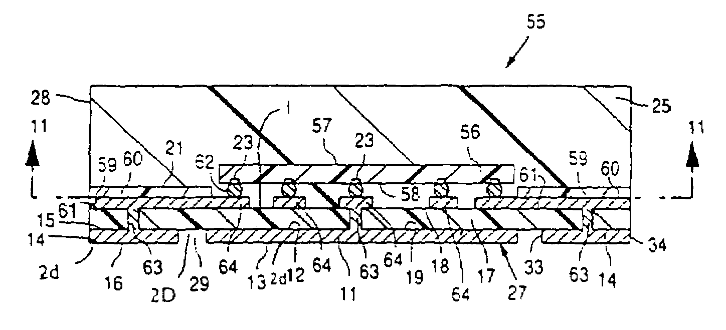
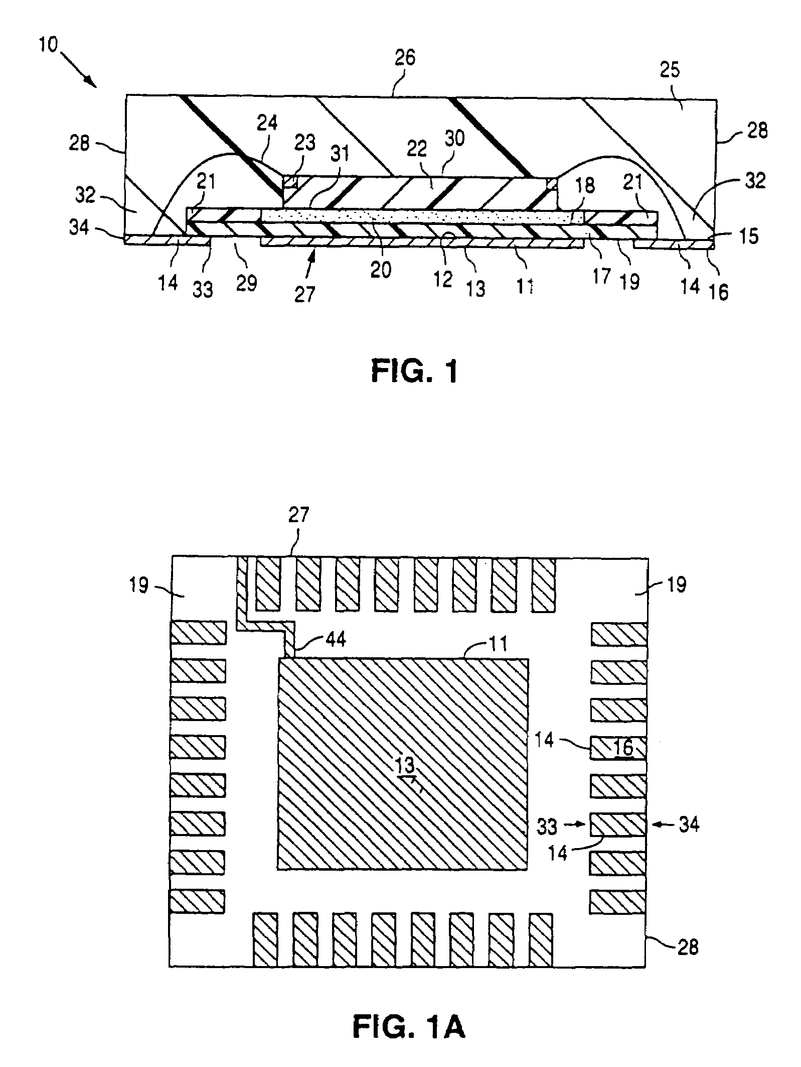
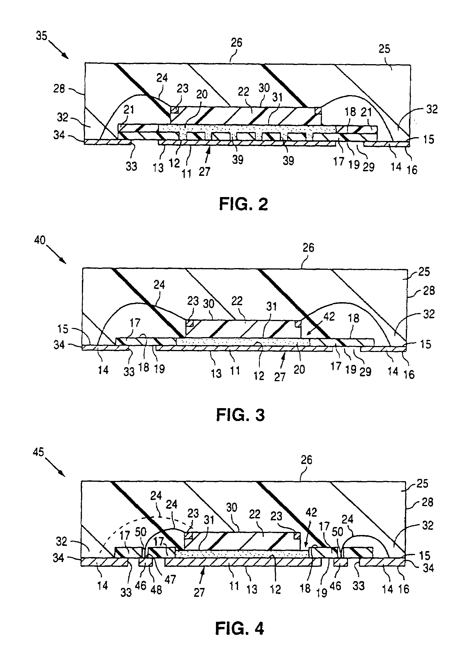
[0025]Similar features in the various figures are identified using the same reference numbers, and redundant discussion is omitted.

[0026]FIG. 1 depicts an embodiment of a package 10 within the present invention. Package 10 includes a package body formed in an insulative encapsulant material 25. Package 10 includes an upper exterior first surface 26, an opposite lower exterior second surface 27, and orthogonal exterior side surfaces 28 between first surface 26 and second surface 27.

[0027]Lower second surface 27 of package 10 includes an exposed planar metal die pad 11 and exposed planar metal leads 14. Die pad 11 includes a planar upper first surface 12 and an opposite planar lower second surface 13. Leads 14 each include a planar upper first surface 15 and a planar lower second surface 16. Leads 14 are in the same horizontal plane as die pad 11.

[0028]Leads 14 of package 10 of FIG. 1 extend laterally on lower surface 27 from package side 28 toward die pad 11. In particular, leads 14 ...


PUM


Abstract

Integrated circuit device packages and substrates for making the packages are disclosed. One embodiment of a substrate includes a planar sheet of polyimide having a first surface, an opposite second surface, and apertures between the first and second surfaces. A planar metal die pad and planar metal are attached to the second surface of the polyimide sheet. The apertures in the polyimide sheet are juxtaposed to the leads. A package made using the substrate includes an integrated circuit device mounted above the first surface of the polyimide sheet opposite the die pad. Bond wires are connected between the integrated circuit device and the leads through the apertures in the polyimide sheet. An encapsulant material covers the first surface of the polyimide sheet, the integrated circuit device, the bone wires, and the apertures. The die pad and leads are exposed at an exterior surface of the package.

Description

CROSS-REFERENCE TO RELATED APPLICATION[0001]The present application is a continuation of U.S. application Ser. No. 10 / 354,772 entitled INTEGRATED CIRCUIT DEVICE PACKAGES AND SUBSTRATES FOR MAKING THE PACKAGES filed Jan. 30, 2003 now U.S. Pat. No. 6,833,609, which is a continuation of U.S. application Ser. No. 09 / 434,589 entitled INTEGRATED CIRCUIT DEVICE PACKAGES AND SUBSTRATES FOR MAKING THE PACKAGES filed Nov. 5, 1999 now U.S. Pat. No. 6,580,159.FIELD OF THE INVENTION[0002]The present invention concerns packages for an integrated circuit device, substrates for making such packages, and methods of making the packages and substrates.BACKGROUND OF THE INVENTION[0003]U.S. Pat. No. 5,859,475 to Freyman et al. describes several ball grid array style packages for an integrated circuit device. The packages include a thin planar polyimide sheet. In one embodiment, a die pad and metal traces are formed on the upper surface of the polyimide sheet. An integrated circuit device is mounted on t...

Claims


Application Information

Patent Timeline
IPC IPC(8): H01L23/495H01L23/31H01L23/498
CPCH01L23/3121H01L23/66H01L24/97H01L24/28H01L24/48H01L2224/16H01L2224/48091H01L2224/48195H01L2224/48228H01L2224/49171H01L2224/97H01L2924/01013H01L2924/01027H01L2924/01029H01L2924/01075H01L2924/01078H01L2924/01079H01L2924/01082H01L2924/078H01L2924/14H01L2924/19015H01L2924/19041H01L2924/19042H01L2924/19107H01L2924/30107H01L2924/3011H01L2924/00014H01L2224/85H01L2224/81H01L24/49H01L2924/01006H01L2924/01024H01L2924/01033H01L2224/73265H01L2224/32225H01L2224/48227H01L2224/16225H01L2924/00H01L24/45H01L2224/45144H01L2224/45147H01L2924/00012H01L23/4985H01L24/32H01L2224/27013H01L2224/32057H01L2224/83051H01L2224/83385H01L2224/2919H01L2224/83192H01L2924/01028H01L2224/32013H01L2224/16235H01L2224/05571H01L2224/05573H01L2924/181H01L24/73H01L2224/40H01L2224/83H01L2924/0665H01L2224/05599H01L2224/45H01L2224/48H01L2224/49
Inventor FUSARO, JAMES M.DARVEAUX, ROBERT F.RODRIGUEZ, PABLO
Owner AMKOR TECH SINGAPORE HLDG PTE LTD
Learn More