Digital DC-offset correction circuit for an RF receiver

a dc offset and receiver technology, applied in the field of rf receivers, can solve the problems of long-term expected value of input data that must be zero, functional error in decimation filter, integrator saturation,

Active Publication Date: 2007-05-22
NAT SEMICON CORP
View PDF13 Cites 20 Cited by
  • Summary
  • Abstract
  • Description
  • Claims
  • Application Information

AI Technical Summary

Problems solved by technology

However, a problem associated with the decimation filter employing a chain of integrators is that the long-term expected value of input data must be zero.
Even a minor DC offset in the input data may cause saturation of the integrators and a functional error in the decimation filter.
Unfortunately, many of the analog circuits in the receive path preceding the decimation filter generate DC-offset voltages, either individually or by combined effect.

Method used


Image

  • Digital DC-offset correction circuit for an RF receiver
  • Digital DC-offset correction circuit for an RF receiver
  • Digital DC-offset correction circuit for an RF receiver

Examples


Embodiment Construction

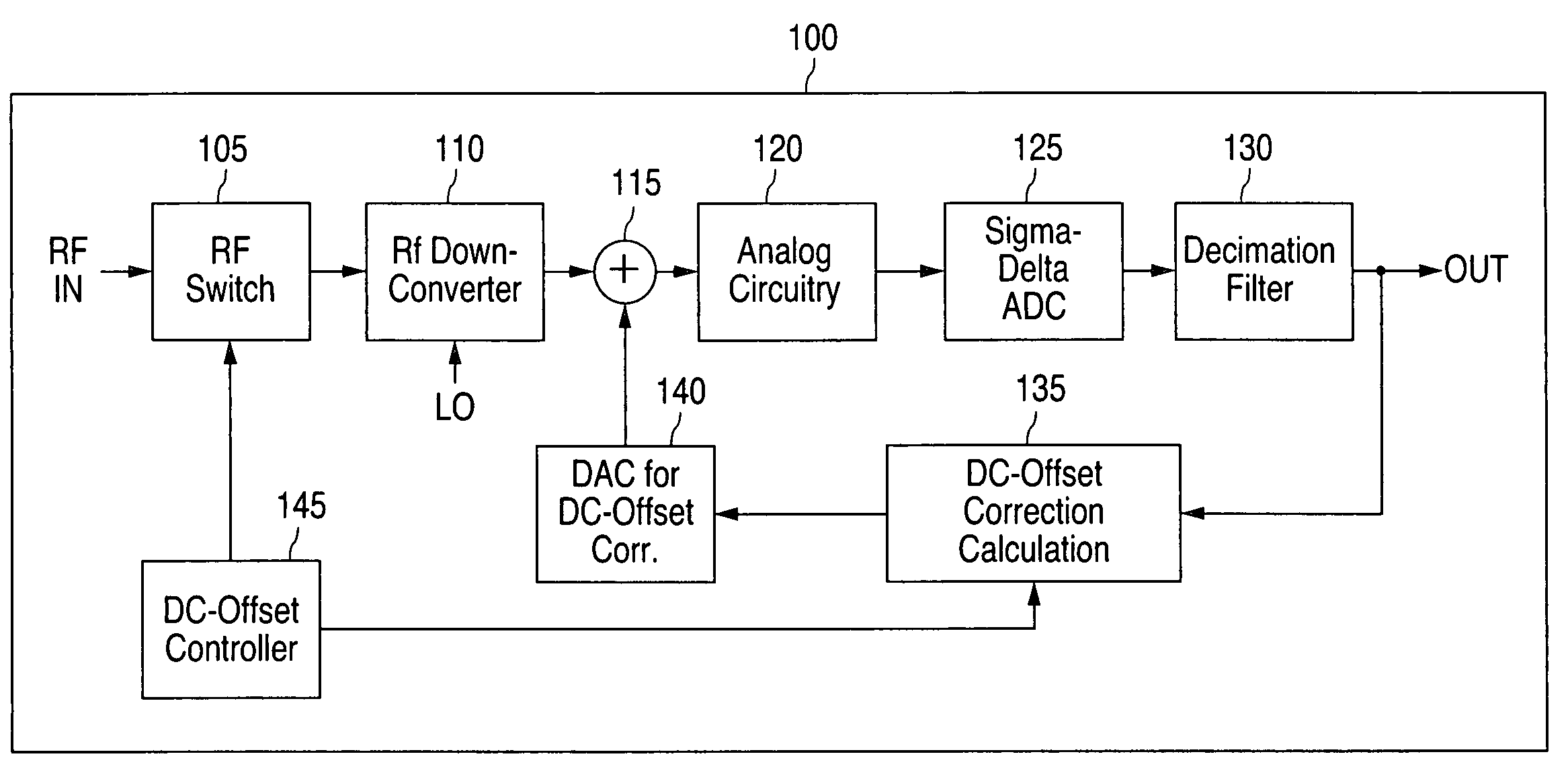
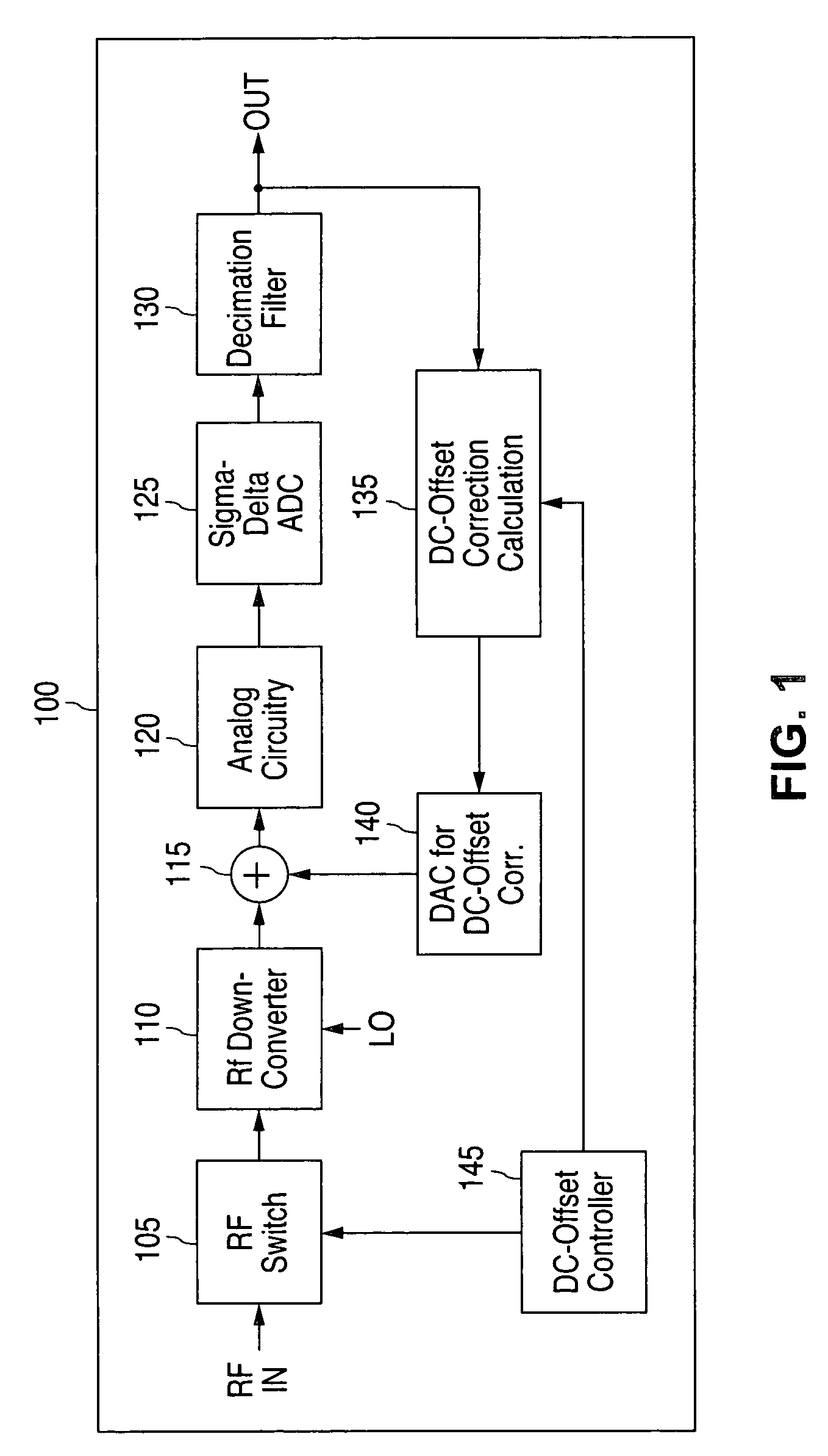
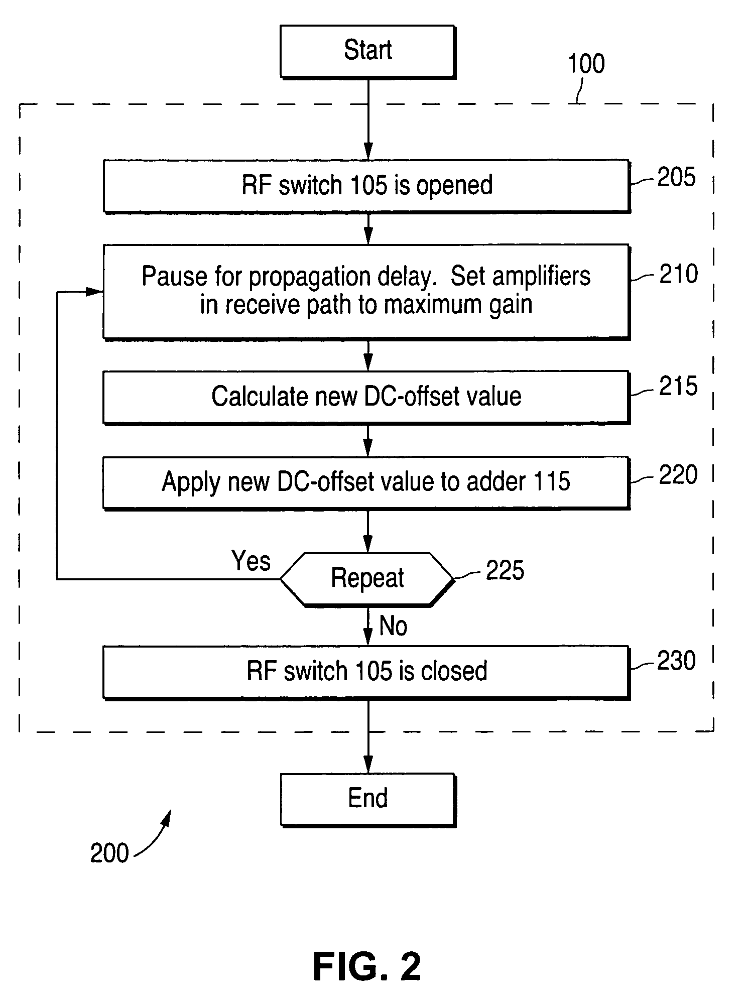
[0017]FIGS. 1 and 2, discussed below, and the various embodiments used to describe the principles of the present invention in this patent document are by way of illustration only and should not be construed in any way to limit the scope of the invention. Those skilled in the art will understand that the principles of the present invention may be implemented in any suitably arranged radio frequency (RF) receiver.

[0018]FIG. 1 illustrates exemplary radio frequency (RF) receiver 100, which incorporates a direct current (DC)-offset correction circuit according to an exemplary embodiment of the present invention. RF receiver 100 comprises radio frequency (RF) switch 105, radio frequency (RF) down-converter 110, adder 115, analog circuitry 120, sigma-delta analog-to-digital converter (ADC) 125, and decimation filter 130. RF receiver 100 further comprises DC-offset correction circuitry comprising DC-offset correction calculation block 135, digital-to-analog converter (DAC) for DC-offset cor...


PUM


Abstract

An RF receiver comprising a radio-frequency (RF) down-converter for receiving and down-converting an input RF signal to a lower frequency analog signal (e.g., an IF signal or baseband signal) and analog processing circuitry for receiving the lower frequency analog signal from the RF down-converter and outputting a processed analog signal. The processed analog signal includes a DC-offset signal introduced by the RF down-converter and the analog processing circuitry. The RF receiver also comprises an ADC circuit for converting the processed analog signal to a sequence of digital samples and a DC-offset correction circuit for detecting the DC-offset signal in a digital output signal of the RF receiver. The DC-offset correction circuit adds a DC-offset correction signal to the lower frequency analog signal. Adding the DC-offset correction signal to the lower frequency analog signal reduces the DC-offset signal in the processed analog signal at the analog processing circuitry output.

Description

TECHNICAL FIELD OF THE INVENTION[0001]The present invention is generally directed to radio frequency (RF) receivers and, in particular, to a DC offset correction circuit for use in an RF receiver.BACKGROUND OF THE INVENTION[0002]In order to get high performance in a conventional radio frequency (RF) receiver, it is often required that the input signals to internal components in the RF receive path be centered on zero volts (0 V). Even a small direct current (DC) offset voltage at the input of a component may have a large effect on the dynamic range of the component.[0003]For example, many RF receivers comprise an analog-to-digital converter (ADC) that converts an analog pass band signal by using a high sampling frequency. One common ADC component comprises a sigma-delta (ΣΔ) modulator block followed by a decimation filter block. After the A / D conversion, the frequency of the pass band signal is decreased to the level of the base band, but the sampling frequency still remains high. E...

Claims


Application Information

Patent Timeline
Patent Type & Authority Patents(United States)
IPC IPC(8): H04B7/00H04B1/06H04B1/16
CPCH04B1/30H04L25/063
Inventor GRASBECK, ARI JUHANISPORRON, MIKAEL
Owner NAT SEMICON CORP
Why Eureka
Try Eureka