Shift register and image display device
a technology of image display device and shift register, which is applied in the direction of instruments, static indicating devices, etc., can solve the problems of bulky driving circuit, tendency to reduce the driving voltage as small as possible, and erroneous image data to be outputted to the data signal line, etc., to achieve narrower frame width and simplified driving circuit
- Summary
- Abstract
- Description
- Claims
- Application Information
AI Technical Summary
Benefits of technology
Problems solved by technology
Method used
Image

Examples
embodiment 1
[Embodiment 1]
[0091]The following description will discuss one embodiment of the present invention.
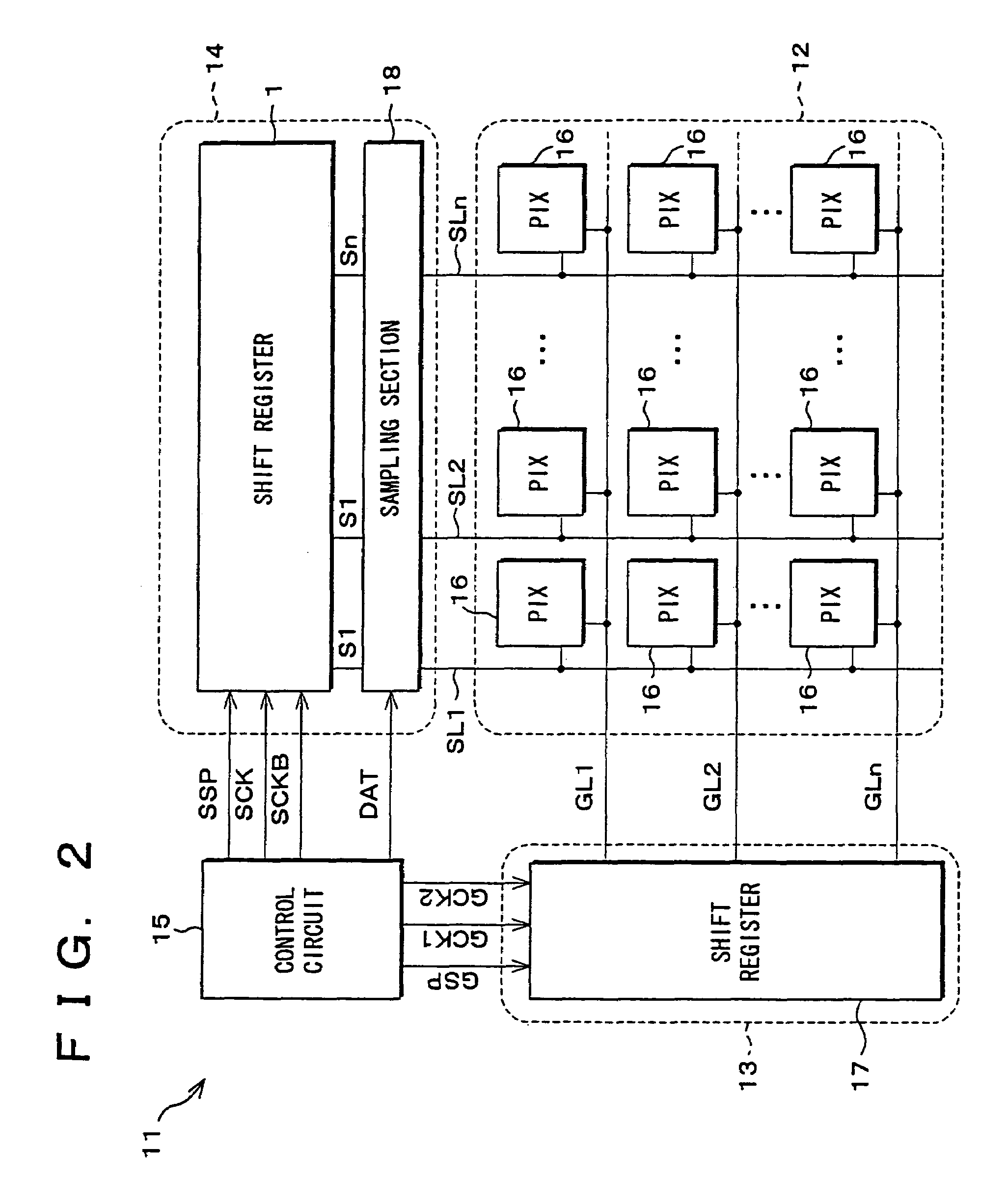
[0092]The shift register of the present invention is preferably applied to a data signal line driving circuit and a scanning signal line driving circuit of an image display device; however, the shift register can also be applied to apparatuses other than the image display device. In the following description, the shift register that is related to the embodiment of the present invention and that is applied to a data signal line driving circuit will be explained as Embodiment 1, and the shift register that is related to the embodiment of the present invention and that is applied to a scanning signal line driving circuit will be explained as Embodiment 2.
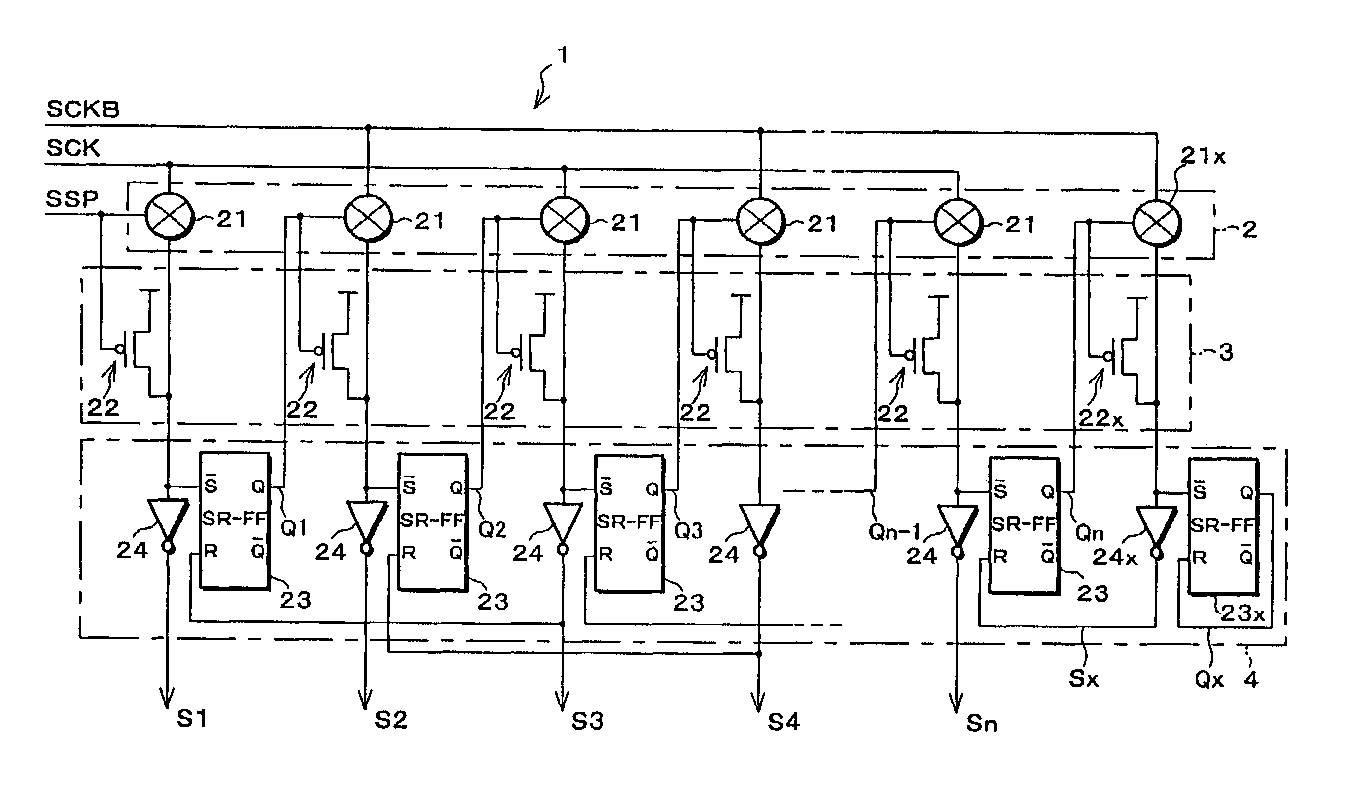
[0093]As illustrated in FIG. 1, the shift register 1 of the present embodiment, which is schematically constituted by a switch section 2, an input stability section 3 and a flip-flop section 4, is used as, for example, a data signal line ...
embodiment 2
[Embodiment 2]
[0141]Referring to FIGS. 13 and 14, the following description will discuss the second embodiment of the present invention. Here, in the present embodiment, those members that have the same functions and that are described in Embodiment 1 are indicated by the same reference numerals, and the description thereof is omitted.
[0142]As described earlier, the shift register 17 of the present embodiment is a shift register that is used in the scanning signal line driving circuit 13. As illustrated in FIG. 13, the shift register 17 has the same construction as the shift register 1 of Embodiment 1 except that two kinds of clock signals GCK1 and GCK2 are inputted thereto, and that the start pulse GSP is inputted as a start pulse.
[0143]As illustrated in FIG. 14, the clock signals GCK1•GCK2 have such phases that the respective low-level periods are not overlapped with each other; that is, their phases are offset from each other by 180°. Each of the clock signals GCK1 and GCK2 is se...
embodiment 3
[Embodiment 3]
[0148]Referring to FIGS. 15 and 16(a) through 16(k), the following description will discuss the third embodiment of the present invention. Here, in the present embodiment, those members that have the same functions and that are described in Embodiments 1 and 2 are indicated by the same reference numerals, and the description thereof is omitted.
[0149]The image display device of the present embodiment has the same structure as the image display device 11 explained in Embodiment 1 except that the scanning signal line driving circuit 13 and the data signal line driving circuit 14 are formed on the same substrate constituted by a plurality of pixels 16 and the display device 12.
[0150]In other words, in the image display device of the present embodiment, the scanning signal line driving circuit 13 and the data signal line driving circuit 14 are formed on an insulating substrate, that is, for example, a glass substrate 41 (driver monolithic construction), together with the, d...
PUM
 Abstract
Description
Claims
Application Information
 - R&D Engineer
- R&D Manager
- IP Professional
- Industry Leading Data Capabilities
- Powerful AI technology
- Patent DNA Extraction
Browse by: Latest US Patents, China's latest patents, Technical Efficacy Thesaurus, Application Domain, Technology Topic.
© 2024 PatSnap. All rights reserved.Legal|Privacy policy|Modern Slavery Act Transparency Statement|Sitemap