Electronic parts built-in substrate and method of manufacturing the same
a technology of built-in substrates and electronic parts, which is applied in the association of printed circuit non-printed electric components, solid-state devices, semiconductor devices, etc., can solve the problems of reducing the reliability of the electric bonding applied to flip-chip bonding the upper semiconductor chip to the wiring, prone to defocus in photolithography, and difficult to form wiring patterns on the insulating film with good precision. , to achieve the effect of reducing production costs and high crack resistan
- Summary
- Abstract
- Description
- Claims
- Application Information
AI Technical Summary
Benefits of technology
Problems solved by technology
Method used
Image

Examples
embodiment
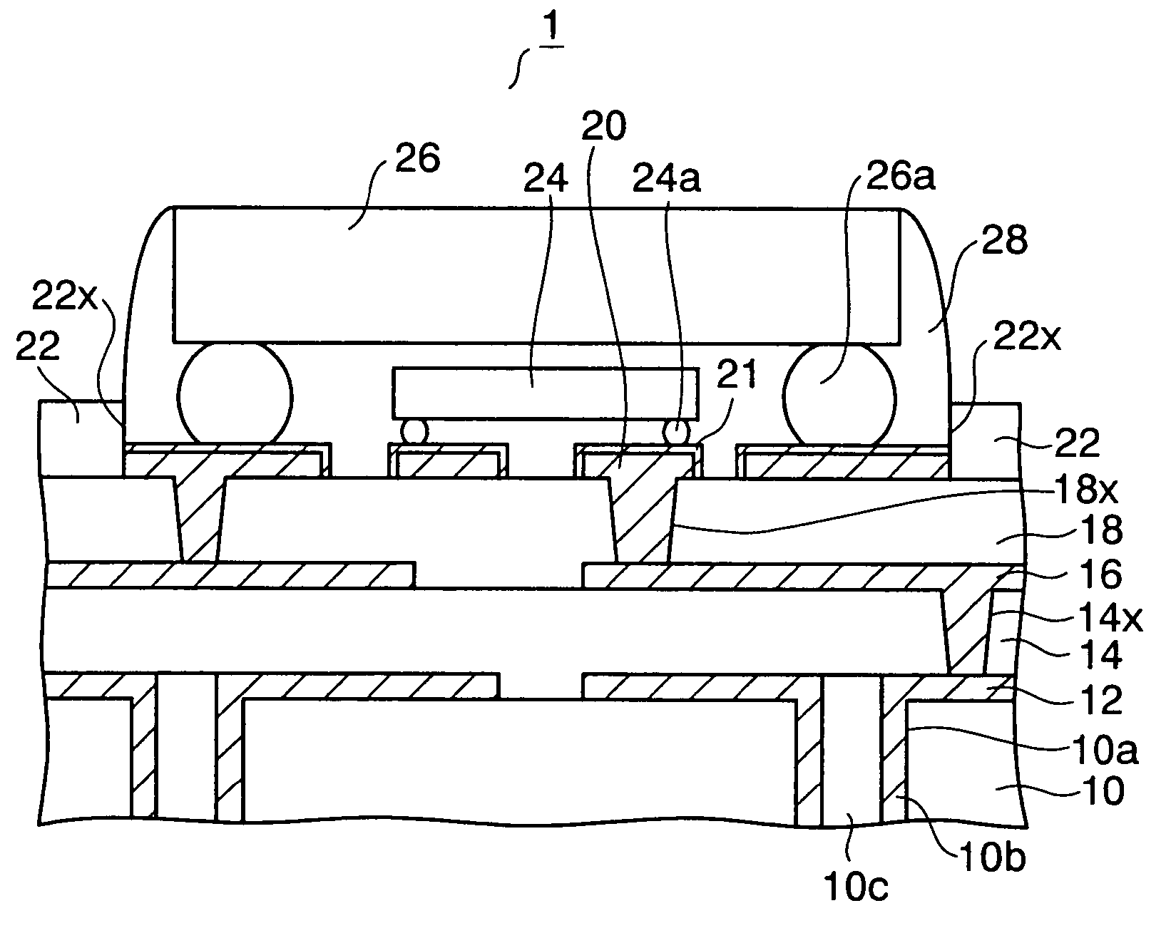
[0043](Embodiment)
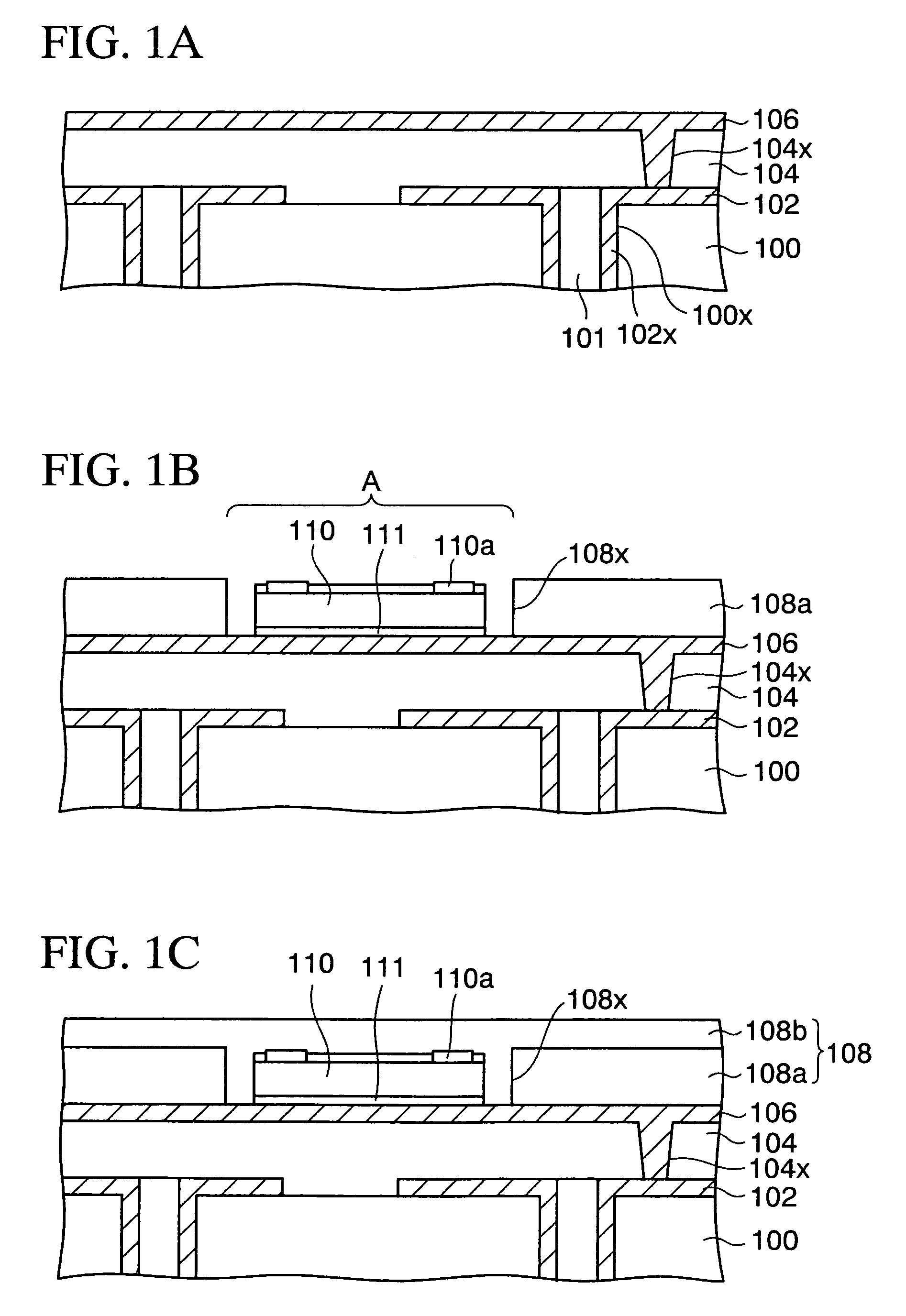
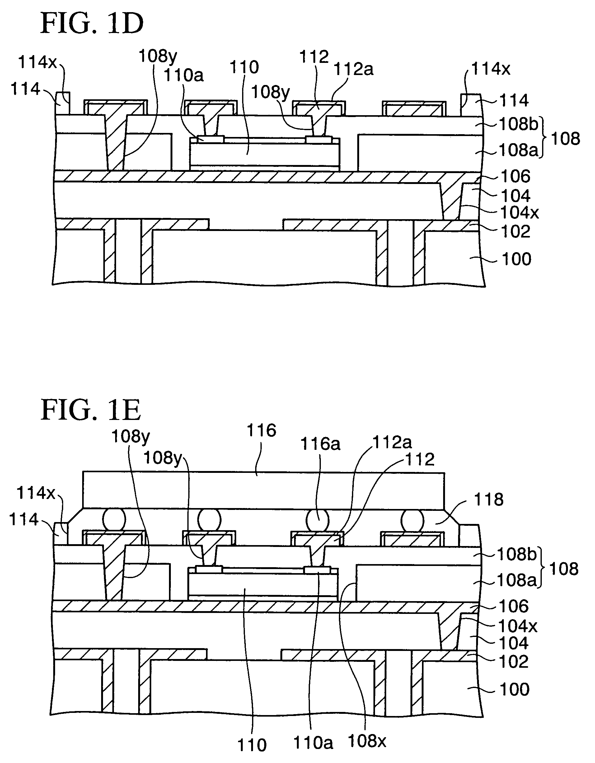
[0044]FIGS. 3A to 3H are sectional views showing a method of manufacturing an electronic parts built-in substrate according to an embodiment of the present invention in order. As shown in FIG. 3A, first a base substrate 10 is prepared to manufacture a build-up wiring substrate. This base substrate 10 is made of insulating material such as glass epoxy resin, or the like. Through holes 10a are provided in the base substrate 10, then a through-hole plating layer 10b connected to a first wiring pattern 12 on the base substrate 10 respectively is formed on inner surfaces of the through holes 10a, and then the openings are buried with a resin body 10c.
[0045]Then, as shown in FIG. 3B, a first interlayer insulating film 14 is formed on the first wiring patterns 12. As the first interlayer insulating film 14, a resin such as epoxy resin, polyimide resin, polyphenylene ether resin, or the like may be employed. As an example of the forming method, a resin film is formed by l...
PUM
 Abstract
Description
Claims
Application Information
 - R&D
- Intellectual Property
- Life Sciences
- Materials
- Tech Scout
- Unparalleled Data Quality
- Higher Quality Content
- 60% Fewer Hallucinations
Browse by: Latest US Patents, China's latest patents, Technical Efficacy Thesaurus, Application Domain, Technology Topic, Popular Technical Reports.
© 2025 PatSnap. All rights reserved.Legal|Privacy policy|Modern Slavery Act Transparency Statement|Sitemap|About US| Contact US: help@patsnap.com