
AC coupling circuit having a large capacitance and a good frequency response

a technology of ac coupling circuit and capacitance, applied in the direction of waveguides, sustainable manufacturing/processing, final product manufacturing, etc., can solve the problems of reflection, loss and deterioration of the signal transmitted thereon, dc level of precedent amplifiers that are often mismatched, etc., to reduce loss and reflection of signals, and maintain the quality of transmitted high frequency signals.

Active Publication Date: 2007-03-27
SUMITOMO ELECTRIC IND LTD
View PDF15 Cites 3 Cited by
  • Summary
  • Abstract
  • Description
  • Claims
  • Application Information

AI Technical Summary

Benefits of technology

The solution improves signal quality by reducing signal loss and reflection across a wide frequency range, maintaining high frequency signal integrity and minimizing parasitic inductance effects.

Problems solved by technology

For example, in the case that two amplifier are serially connected, the output DC level of the precedent amplifier often mismatches to the input DC level of the succeeding one.
This causes a reflection, loss and deterioration of the signal transmitted thereon.

Method used


Image

  • AC coupling circuit having a large capacitance and a good frequency response
  • AC coupling circuit having a large capacitance and a good frequency response
  • AC coupling circuit having a large capacitance and a good frequency response

Examples


fourth embodiment

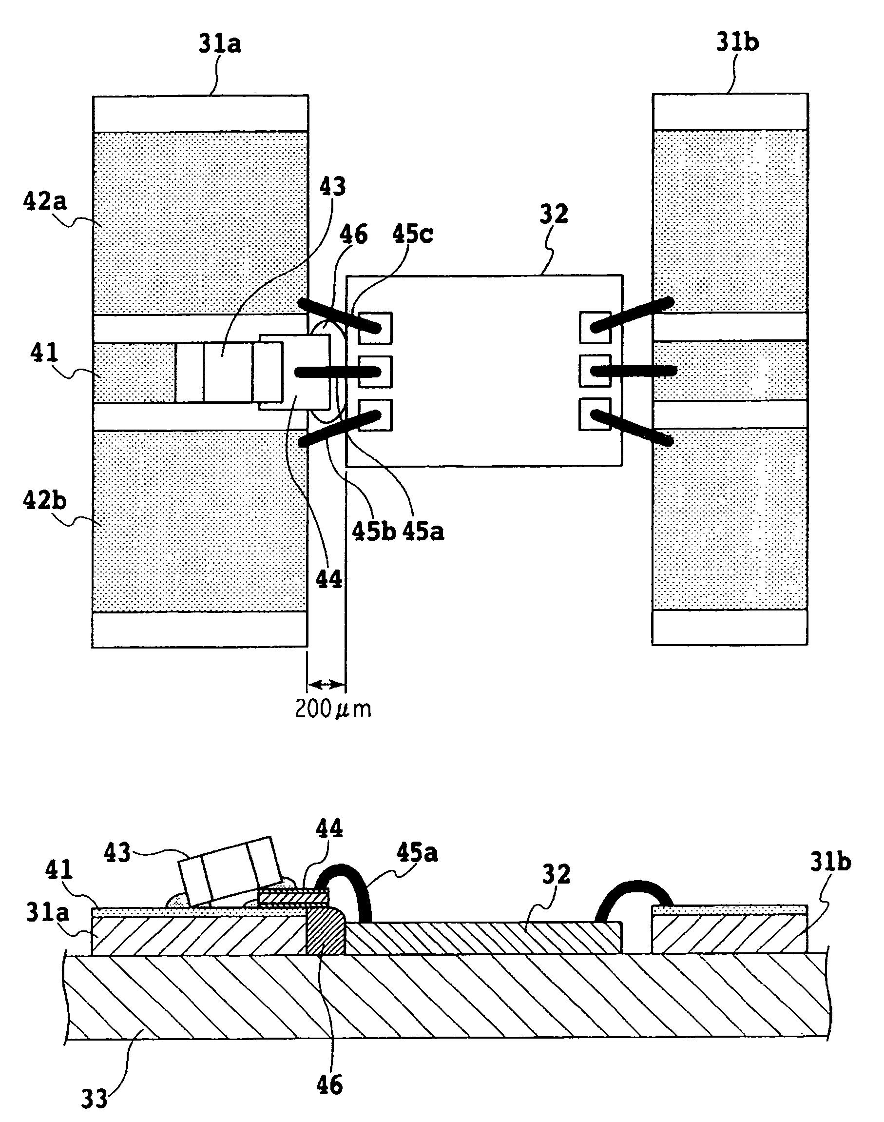
[0035]FIG. 8 is a plan view showing the present invention. The coupling circuit shown in FIG. 8 comprises a ceramic substrate 31 and the bare chip IC 32. On the ceramic substrate 31, a co-planar line, which has a signal line 41 and a pair of ground patterns 42a and 42b sandwiching the signal line therebetween, is formed. The die capacitor 44 is arranged at the edge of the signal line with one electrode thereof facing to the signal line 41, while the other terminal of the die capacitor 44 is wire-bonded to the bare chip IC 32. The edge of the die capacitor 44 is sticking out from the edge of the substrate 31 toward the IC 32. The chip-capacitor 43 is assembled such that the one electrode thereof directly soldered to the signal line 41 and the other electrode is soldered to the upper electrode of the die capacitor 44. Thus, two capacitors 43 and 44, and the co-planar line 41 constitute a coupling circuit.

[0036]As described with referring to FIG. 2, discontinuity points in mechanical a...

fifth embodiment

[0037]FIG. 9 is the present invention. FIG. 9A is a plan view of the coupling circuit that comprises a ceramic substrate 31 and a bare chip IC 32 enclosed in a metal package. FIG. 9B is an equivalent circuit diagram of the coupling circuit shown in FIG. 9A. A co-planar line having a signal line 41 and a pair of ground patterns 42a and 42b sandwiching the signal line 41 with a predetermined gap are formed on the substrate 31. On the edge of the signal line 41, a die capacitor 44 is assembled such that one electrode thereof is facing to the signal line 41. Another electrode of the die capacitor 44 is wire-bonded to the bare chip IC 32. The edge of the die capacitor 44 is sticking out from the edge of the substrate 31. The chip capacitor 43 is assembled such that the one electrode thereof is connected to the signal line 41, while the other electrode thereof is soldered to the upper electrode of the die capacitor 44. Thus, two capacitors 43 and 44 constitute the coupling circuit.

[0038]O...


PUM


Abstract

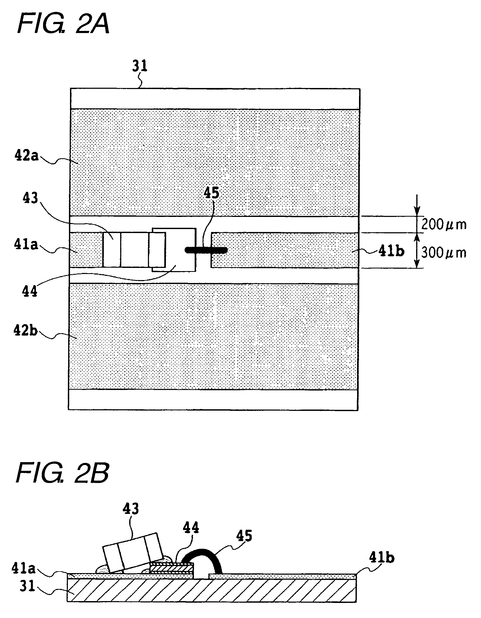
This invention is directed to reduce degradation, loss, and reflection of high frequency signals of a coupling circuit for an alternating current. The coupling circuit, for connecting a first circuit element to a second circuit element, comprises a die capacitor and a chip capacitor connected in parallel to each other. The die capacitor has a first electrode that faces to and is in contact with the first circuit element, and a second electrode that is wire-bonded to the second circuit element. The chip capacitor also has a first electrode that is in contact with the first circuit element and a second electrode that is in contact with the second electrode of the die capacitor. The coupling circuit may show both advantages of superior performance at high frequencies attributed to the die-capacitor and relative large capacitance attributed to the chip-capacitor.

Description

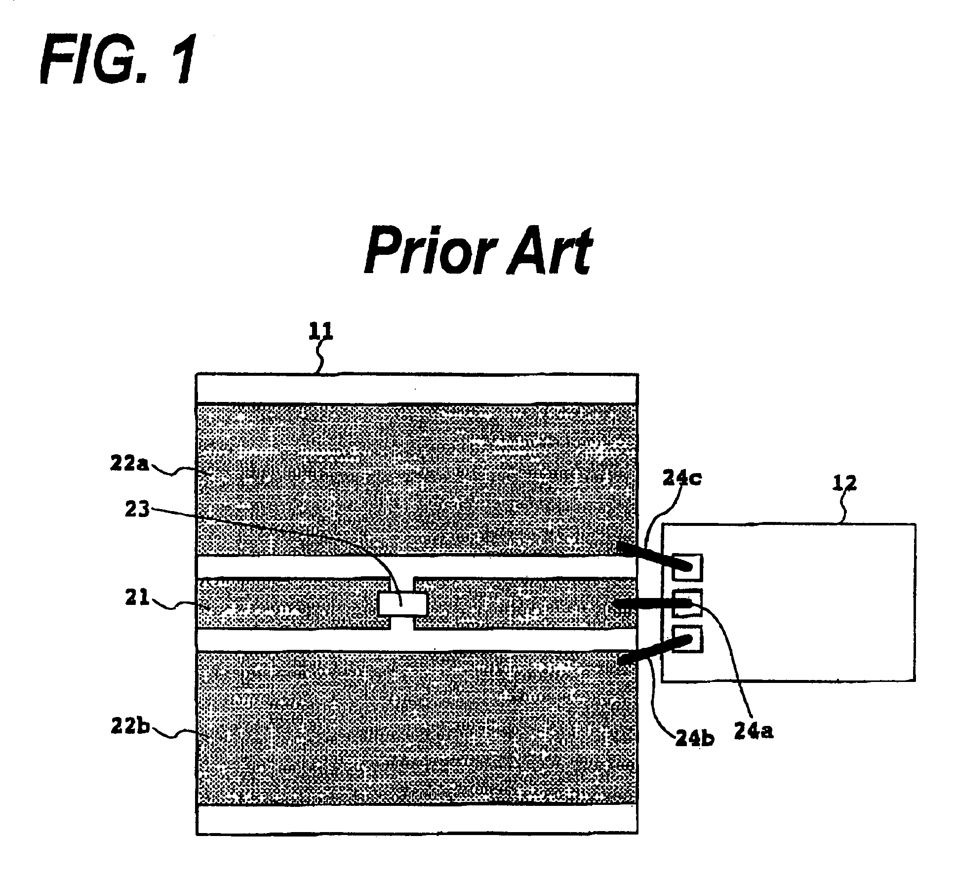
BACKGROUND OF THE INVENTION[0001]1. Field of the Invention[0002]The present relates to an alternating current (AC) circuit, especially, relates to an AC circuit in which a capacitor is used for electrically connecting circuit elements.[0003]2. Related Prior Art[0004]An AC circuit operating in a high frequency band uses specific circuit elements such as transmission line types of a micro-strip and a co-planar, and a passive element with a chip shape. In order to electrically connect active elements, such as an amplifier, the AC coupling circuit must be set between them because direct current (DC) levels of these active elements are different to each other. For example, in the case that two amplifier are serially connected, the output DC level of the precedent amplifier often mismatches to the input DC level of the succeeding one. The AC coupling circuit generally includes a coupling capacitor set on the transmission line connecting the preceding circuit to the succeeding one.[0005]FI...

Claims


Application Information

Patent Timeline
Patent Type & Authority Patents(United States)
IPC IPC(8): H05K7/02H05K7/06H05K7/08H05K7/10H01L23/66H01P1/00H01P1/04H01P1/20H01P3/08H01P5/02H03H7/38H05K1/02
CPCH01L23/66H01L24/49H01P1/047H01P1/2007H05K1/0231H01L2924/014H01L2223/6627H01L2223/665H01L2224/45144H01L2224/48091H01L2224/49171H01L2924/01004H01L2924/01005H01L2924/01006H01L2924/01027H01L2924/01079H01L2924/14H01L2924/15153H01L2924/1517H01L2924/1903H01L2924/19041H01L2924/19042H01L2924/19105H01L2924/30105H01L2924/30107H01L2924/3011H05K1/0219H05K2201/1053H05K2201/10636H05K2201/10643H05K2203/049H01L24/45H01L2924/01033H01L24/48H01L2924/00014H01L2924/15787Y02P70/50H01L2924/00
Inventor KATSUYAMA, TOMOKAZU
Owner SUMITOMO ELECTRIC IND LTD
Learn More