Chip-type electronic component and chip resistor

a technology of electronic components and resistors, applied in the direction of resistor details, resistors adapted for applying terminals, resistive material coatings, etc., can solve the problems of difficult to recognize the application state of conductive paste by checking the appearance, and difficult to check the application state of conductive paste. , to achieve the effect of improving the mass production feasibility of chip electronic components and high speed

Inactive Publication Date: 2007-01-09
PANASONIC CORP
View PDF8 Cites 4 Cited by
  • Summary
  • Abstract
  • Description
  • Claims
  • Application Information

AI Technical Summary

Benefits of technology

[0011]A chip electronic component comprises a substrate and side electrodes disposed at both ends of the substrate, and the entire surface of the side electrode has a lightness not more than 6. According to the chip electronic component, the entire surface of side electrode has a lightness of not more than 6 as defined-in JIS-Z8721. By this configuration, a difference in brightness between substrate and side electrode is made clear. As a result, even with a very small-sized chip electronic component, it is possible to recognize the application state of conductive paste at a high speed. Also, it brings about such advantage that the mass production feasibility of chip electronic components may be improved.

Problems solved by technology

However, as conductive powder in the above conductive paste, generally used is flake silver powder that may realize a low resistance at a low content.
Since the white color is very similar to the color of 96 alumina substrate which makes the substrate, it is not easy to check the application state of conductive paste.
That is, even if the application state of conductive paste is defective, it is difficult to recognize by checking the appearance.
However, due to the recent miniaturization of chip electronic components, it is now difficult to recognize the application state of conductive paste by using the above checking method.
That is, if the recognition sensitivity is improved in order to prevent the generation of slightly defective application, it becomes difficult to check the application state of conductive paste since the metallic luster of flake silver powder contained in the paste is very similar to the color of 96 alumina substrate which makes the substrate.

Method used


Image

  • Chip-type electronic component and chip resistor
  • Chip-type electronic component and chip resistor
  • Chip-type electronic component and chip resistor

Examples


example 1

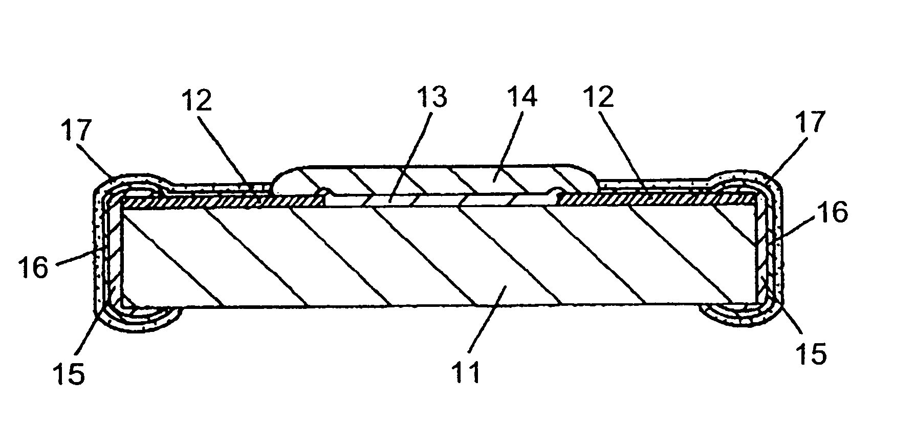
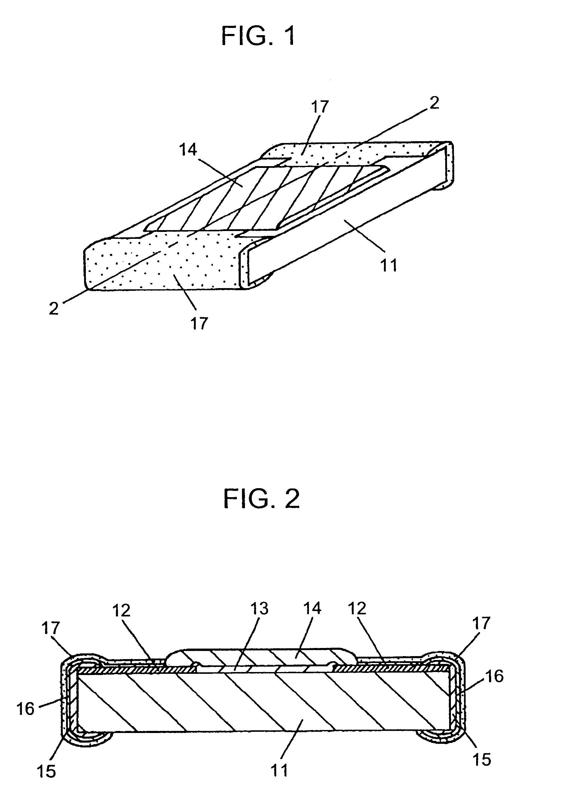
[0041]A structure of a chip resistor in Example 1 of the present invention has the same structure as these of the chip resistor shown in FIG. 1 and FIG. 2. As a resin for the conductive paste for forming side electrodes, bisphenol-A type epoxy resin, a thermosetting resin, and imidazole hardener are used. And spherical silver powder of 0.06 μm in average particle diameter is mixed with the resin at an amount of 85% as spherical conductive particles, and furnace black is further mixed at an amount of 2% as carbon powder.

example 2

[0042]A structure of the chip resistor in Example 2 of the present invention has the same structure as the chip resistor in one embodiment of the present invention shown in FIG. 1 and FIG. 2. As the resin for conductive paste for forming side electrodes, bisphenol-F type epoxy resin, a thermosetting resin, and amine hardener are used. And spherical nickel powder of 2.5 μm in average particle diameter is mixed with the resin at an amount of 90% as spherical conductive particles, and furnace black is further mixed at an amount of 1% as carbon powder.

example 3

[0043]A structure of the chip resistor in Example 3 of the present invention has the same structure as the chip resistor in one embodiment of the present invention shown in FIG. 1 and FIG. 2. As the resin for conductive paste for forming side electrodes, bisphenol-A type epoxy resin, a thermosetting resin, and imidazole hardener are used. And spherical tungsten powder of 10 μm in average particle diameter is mixed with the resin at an amount of 80% as spherical conductive particles, and furnace black is further mixed at an amount of 3% as carbon powder.


PUM


Abstract

In chip electronic components, the application state of conductive paste that makes side electrodes can be optically distinguished in the production of small-sized chip electronic components. The chip electronic component comprises a substrate, and side electrodes disposed at the end portions of the substrate. The lightness of an entire surface of the side electrode is not more than 6 as defined in JIS-Z8721.

Description

[0001]This application is a division of U.S. patent application Ser. No. 10 / 239,617, filed Dec. 12, 2002, now U.S. Pat. No. 7,084,733 B2, issued Aug. 1, 2006, which is a U.S. National Phase Application of PCT International Application PCT / JP02 / 00496, filed Jan. 24, 2002, the contents of which are incorporated herein by reference.TECHNICAL FIELD[0002]The present invention relates to chip electronic components used in various electronic apparatuses, and chip resistors. Particularly, the present invention relates to very small-sized chip electronic components.BACKGROUND ART[0003]Recently, demand for miniaturization or dimensional reduction of electronic apparatuses has increased. As a result, very small-sized chip electronic components are increasingly employed as electronic components. Particularly, very small-sized chip electronic components which are as small as 0.6 mm in length×0.3 mm in width×0.25 mm in thickness are manufactured in recent years.[0004]A conventional chip electroni...

Claims


Application Information

Patent Timeline
Patent Type & Authority Patents(United States)
IPC IPC(8): H01C7/10H01C1/148H01C7/00H01C17/06H01C17/065H01C17/28
CPCH01C1/148H01C17/283H01C17/065H01C7/003
Inventor HARADA, MITSURUOMOYA, KAZUNORIHASHIMOTO, MASATOFUKUOKA, AKIO
Owner PANASONIC CORP
Why Eureka
Try Eureka