
Stressed semiconductor device structures having granular semiconductor material

a semiconductor and granular technology, applied in the direction of semiconductor devices, electrical equipment, transistors, etc., can solve the problems of difficult control of stress properties, and achieve the effects of improving device performance, preventing compressive stress, and improving mobility

Inactive Publication Date: 2006-10-17
GLOBALFOUNDRIES INC
View PDF110 Cites 8 Cited by
  • Summary
  • Abstract
  • Description
  • Claims
  • Application Information

AI Technical Summary

Benefits of technology

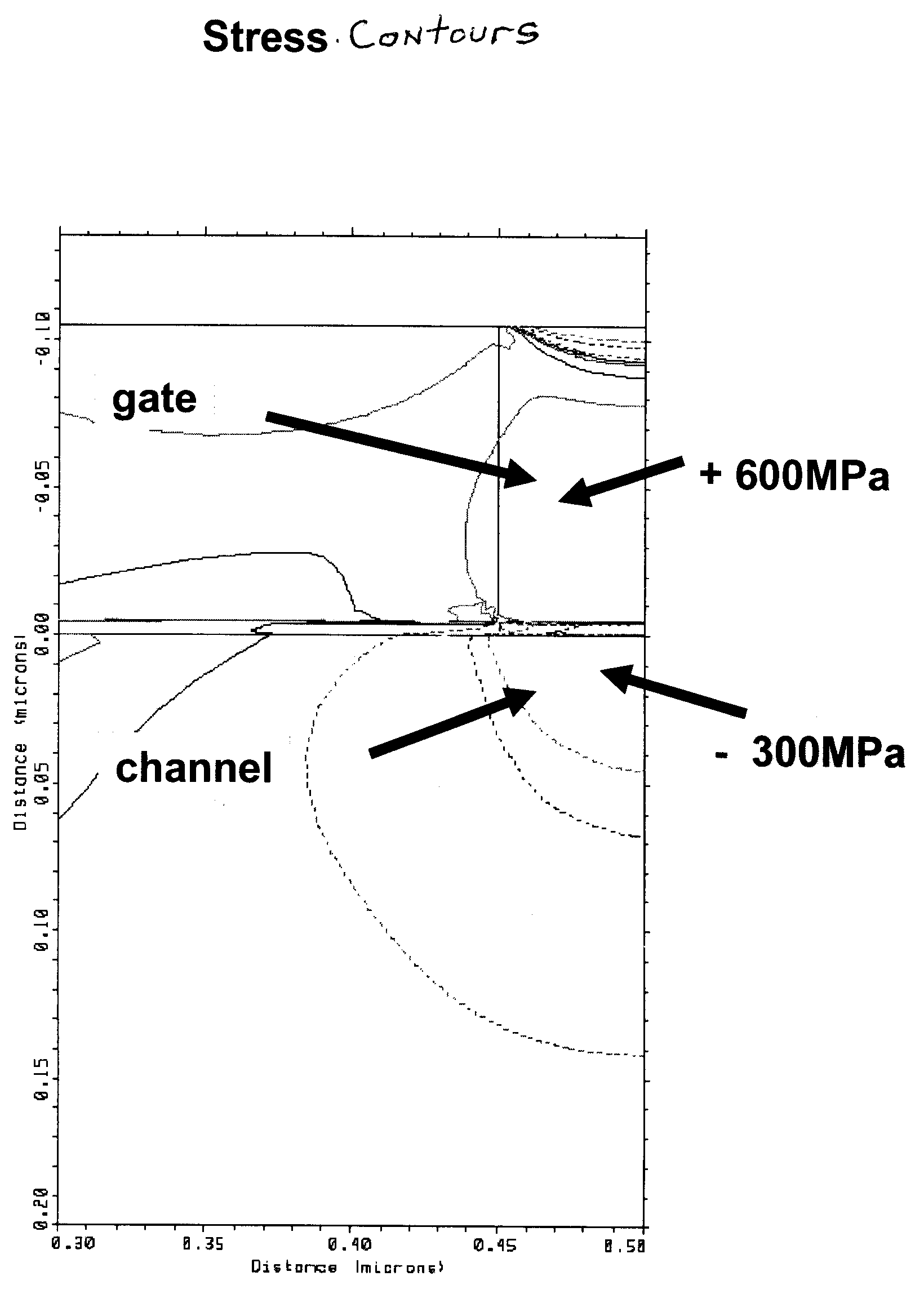
The present invention improves device performance by enhancing channel mobility. This is achieved by using small grain polysilicon to control stress properties, which results in a compressive stress to the pFET channel and a tensile stress to the FET channel. The method includes depositing small grain poly Si films in gate electrode stacks, which become highly tensile as a result of annealing. The resulting semiconductor device structure has improved channel mobility.

Problems solved by technology

Prior to the prevent invention these stress properties were very difficult to control.

Method used


Image

  • Stressed semiconductor device structures having granular semiconductor material
  • Stressed semiconductor device structures having granular semiconductor material
  • Stressed semiconductor device structures having granular semiconductor material

Examples


Embodiment Construction

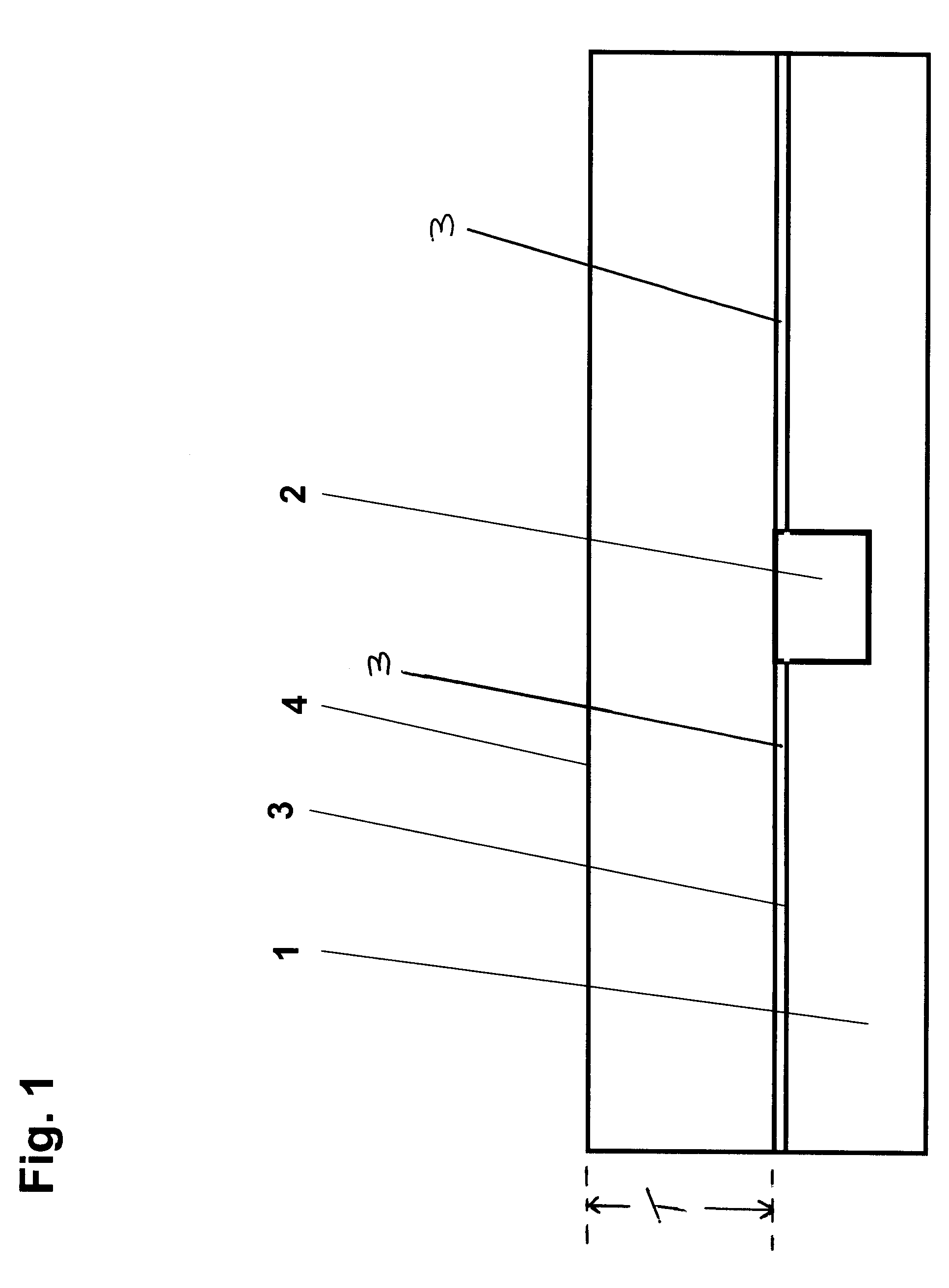
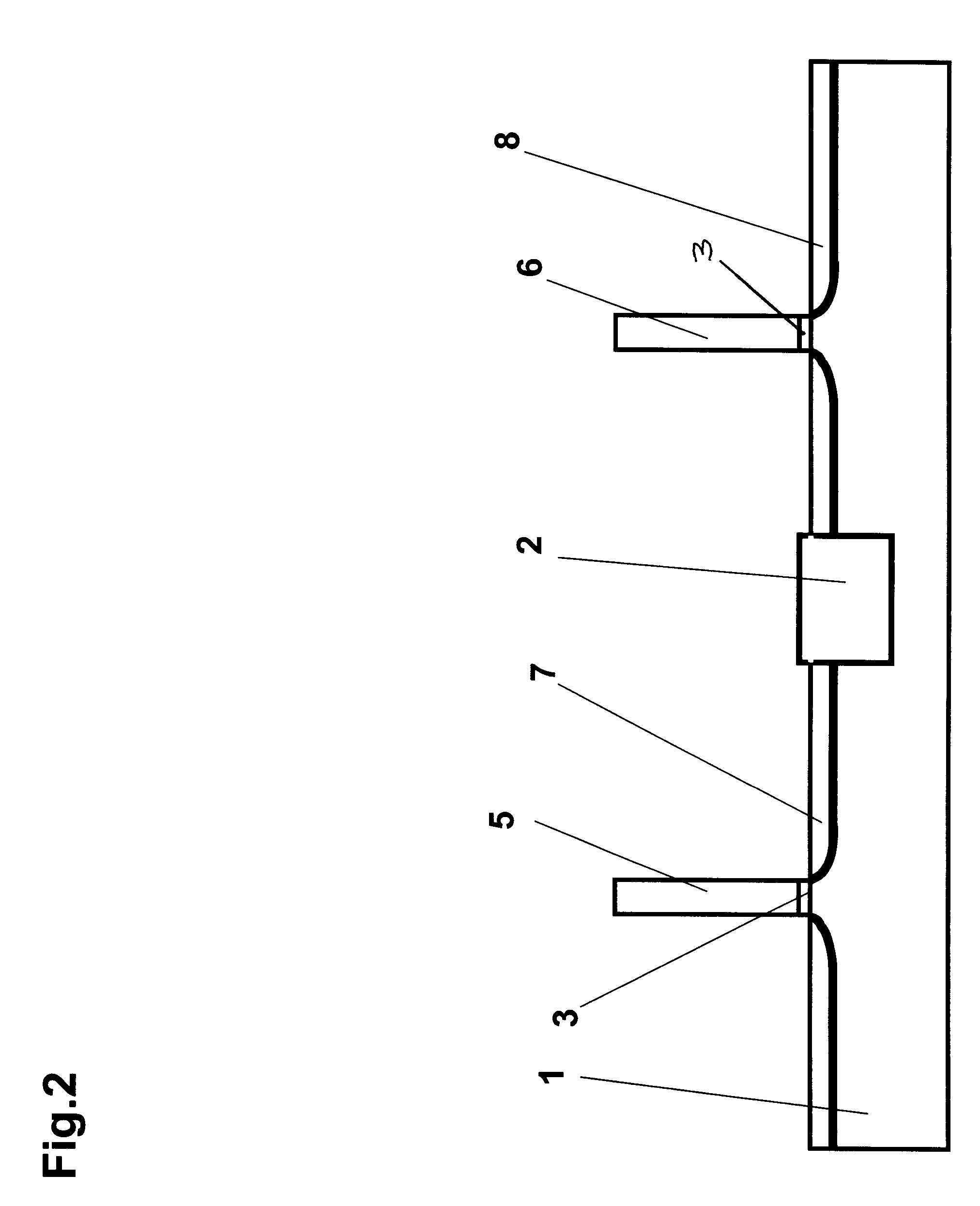
[0010]Turning now to the figures, and FIG. 1 in particular, a semiconductor substrate 1 is provided. The semiconductor substrate is a bulk Si substrate, an SOI substrate, or a stressed (strained) Si substrate. Alternatively, the substrate is a hybrid substrate which includes more than one surface orientation. The substrate alternatively includes a semiconductor material other than Si, such as Ge or any combination of Group III–V elements or Group II–V elements.

[0011]After an initial substrate cleaning procedure (conventional), an isolation scheme is carried out. As is well known in semiconductor manufacturing, the isolation scheme is used to separate selected devices electrically from each other. The isolation scheme may be a standard or a modified shallow trench isolation (STI) scheme. The STI 2 is shown in FIG. 1. Alternatively, the isolation is accomplished using a LOCOS process or mesa isolation scheme, as is well known in the art of fabricating semiconductor devices. For variou...


PUM

PropertyMeasurementUnit
grain sizeaaaaaaaaaa
thicknessaaaaaaaaaa
heightaaaaaaaaaa

Abstract

A method of fabricating a semiconductor device structure, includes: providing a substrate, providing an electrode on the substrate, forming a recess in the electrode, the recess having an opening, disposing a small grain semiconductor material within the recess, covering the opening to contain the small grain semiconductor material, within the recess, and then annealing the resultant structure.

Description

BACKGROUND OF INVENTION[0001]The present invention relates to semiconductor device structures, such as a CMOS device structure including both FET and pFET devices.[0002]Mobility enhancements are important to future semiconductor, e.g. CMOS device technologies. Performance improvements from conventional process technologies are becoming extremely difficult to achieve. Methods to stress Si channels include: using SiGe which imparts stress from the bottom of the channel; different shallow trench isolation (STI) material choices which impart stresses from various sides, and SiN etch stop layers which also impart longitudinal stress from the sides. Drawbacks from the SiGe buffer layer or implanted-anneal-buffer approach with a strained Si cap layer are well known. Drawbacks include dislocations that impact yield severely, along with significant difficulty controlling As diffusion enhancements. Further, the process is quite complicated and costly. The STI approach is less costly but is no...

Claims


Application Information

Patent Timeline
Patent Type & Authority Patents(United States)
IPC IPC(8): H01L29/76H01L29/94H01L31/062H01L31/113H01L31/119H01L21/8238
CPCH01L21/28035H01L21/28247H01L21/324H01L21/823807H01L21/823842H01L29/4925H01L29/66545H01L29/6659H01L29/7845H01L21/26513H01L21/28167H01L29/1083H01L29/517H01L29/665H01L21/2658H01L31/119H01L21/8238H01L21/76
Inventor DORIS, BRUCE BBELYANSKY, MICHAEL PBOYD, DIANE CCHIDAMBARRAO, DURESETIGLUSCHENKOV, OLEG
Owner GLOBALFOUNDRIES INC
Learn More