Optical writing unit, a driving method thereof, and an image forming apparatus

a technology of optical writing unit and drive method, which is applied in the direction of printing, visual presentation, instruments, etc., can solve the problems of difficult uniformity maintenance, difficult to accurately control the distance (gap) between light emitting diode array chips, and the need to re-mount chips on the substrate, etc., to achieve efficient setup

Inactive Publication Date: 2006-06-27
RICOH KK
View PDF23 Cites 27 Cited by
  • Summary
  • Abstract
  • Description
  • Claims
  • Application Information

AI Technical Summary

Benefits of technology

[0022]The present invention provides an optical writing unit that makes vertical stripes appearing on a printing result inconspicuous, which dispenses with the conventional need for re-mounting light emitting device array chips.
[0040]The present invention provides the compensation value for the driving current such that a greater light volume is emitted from the light emitting devices near the edge of the light emitting device array chips when Pa>PH, and a lesser light volume is emitted from the light emitting devices near the edge of the light emitting device array chips when Pa<PL. In this manner, the vertical stripe becomes inconspicuous without complicating the driving circuit.

Problems solved by technology

However, it is difficult to maintain the uniformity in the interval between a light emitting diode on the edge of a light emitting diode-array chip 324 (chip) and another light emitting diode on the adjacent edge of the adjacent chip.
Specifically, it is difficult to accurately control the distance (gap) between the light emitting diode-array chips (the chips) when mounting the chips on the substrate.
For this reason, a conventional problem is that the chips have to be re-mounted on the substrate.
However, these solutions make the driving circuit complicated.
It is desirable that all the light emitting diodes 3 be mounted at the predetermined interval P. However, in fact, the mounting interval of the light emitting diode-array chips 2 cannot be made uniform on the substrate 1, due to mounting errors.
However, in the case of JP,8-118722,A, the adjustment means is needed, and circuit arrangement becomes complicated as the result.
For this reason, it is likely that the adjustment of only the light volume of the light emitting diodes only on the edges of the adjacent light emitting diode-array chips is insufficient to make the-white stripe and the black stripe inconspicuous.
As described above, according to the conventional technology, when a white stripe and black stripe arise in the printing result due to non-uniformity in the distance between the light emitting diodes on the edges of the light emitting diode-array chips, it is necessary to carry out one or any combination of re-mounting the light emitting diode-array chips on the substrate, providing the adjustment means for compensating for the differences in the distances of the light emitting diode-array chips, and providing other means, which complicates the circuit arrangement.

Method used


Image

  • Optical writing unit, a driving method thereof, and an image forming apparatus
  • Optical writing unit, a driving method thereof, and an image forming apparatus
  • Optical writing unit, a driving method thereof, and an image forming apparatus

Examples


example 2

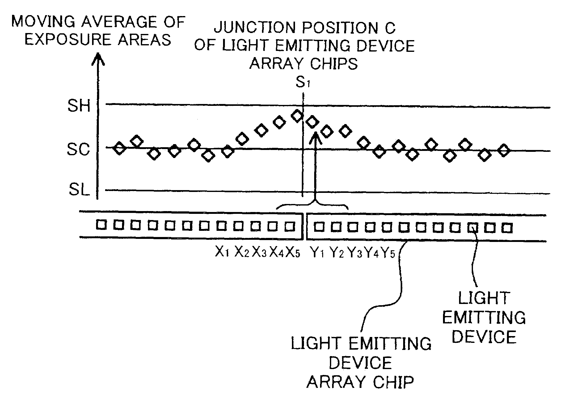
[0119 of the operating process is explained with reference to a flowchart in FIG. 17. In order to obtain a predefined property value concerning the exposure intensity distribution, corresponding to a compensation value, a 2-dimensional exposure intensity distribution is measured using a 2-dimensional CCD, and the likes with each light emitting device irradiating based on the compensation value. Since the light volume changes almost proportionally to the driving current, if an amount of change in the driving current that causes one step of change in the compensation value is known, a change in the light volume corresponding to the step of the compensation value change can be estimated. Although the change in the light volume is almost proportional to the driving current, the constant of proportion is different from light emitting device to light emitting device. Therefore, it is necessary to beforehand measure the constant of each light emitting device. For this purpose, a “probing t...


PUM


Abstract

An optical writing unit is capable of producing a high-quality image in which the formation of white stripes and black stripes, due to uneven intervals between light emitting devices, is suppressed. The unevenness, often occurring at the junction part of two-light emitting diode array chips, is compensated for by increasing or decreasing the light volume of light emitting devices that are located on and near the edge of a light emitting device array chip, such that a property value concerning an exposure intensity distribution falls within a predetermined range for an effective image domain in its entirety.

Description

BACKGROUND OF THE INVENTION[0001]1. Field of the Invention[0002]The present invention generally relates to an optical writing unit, a driving method thereof, and an image forming apparatus that are applicable to digital output equipment, such as a digital copier, a printer, and a digital FAX. The present invention specifically relates to the optical writing unit, the driving method thereof, and the image forming apparatus consisting of a light emitting device array consisting of a plurality of light emitting device array chips, each chip consisting of a plurality of light emitting devices that are arranged at a predetermined interval, and an image forming device array.[0003]2. Description of the Related Art[0004]In recent years and continuing, miniaturization of the optical writing unit for performing digital writing is required as the miniaturization of digital image output equipment, such as a digital copier, a printer, and a digital facsimile, progresses.[0005]Methods of digital ...

Claims


Application Information

Patent Timeline
Patent Type & Authority Patents(United States)
IPC IPC(8): B41J2/45G06K15/12H04N1/04
CPCH04N1/1903G06K15/1247B41J2/45B41J2/451
Inventor MASUDA, KOJI
Owner RICOH KK
Why Eureka
Try Eureka