Infrared absorption measurement method, infrared absorption measurement device, and method of manufacturing semiconductor device
- Summary
- Abstract
- Description
- Claims
- Application Information
AI Technical Summary
Benefits of technology
Problems solved by technology
Method used
Image

Examples
first embodiment
1. First Embodiment
1-1. Infrared Absorption Measurement Device
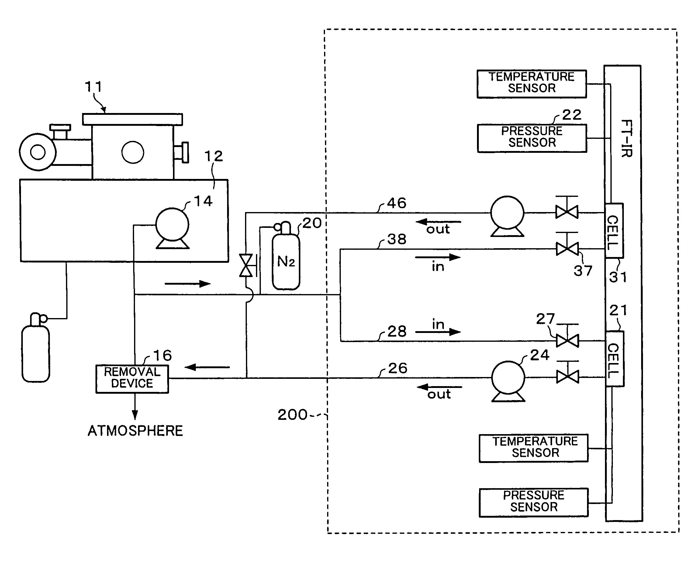
[0085]FIG. 1 schematically shows an infrared absorption measurement device 100 in the present embodiment.
[0086]In the infrared absorption measurement device 100 in the present embodiment, a sample gas including a measurement target component is introduced into an infrared absorption analysis device 10 through a gas inlet line 28, and infrared absorption of the measurement target component is measured by using the infrared absorption analysis device 10. Specifically, the measurement target component included in the sample gas is the target of infrared absorption measurement.
[0087]The sample gas includes at least one measurement target component. In the present embodiment, the case where the sample gas includes one measurement target component (CHF3) is described as an example.
[0088]In the infrared absorption measurement device 100, a valve 27 is provided in the middle of the gas inlet line 28, as shown in FIG. 1. A needle ...
second embodiment
2. Second Embodiment
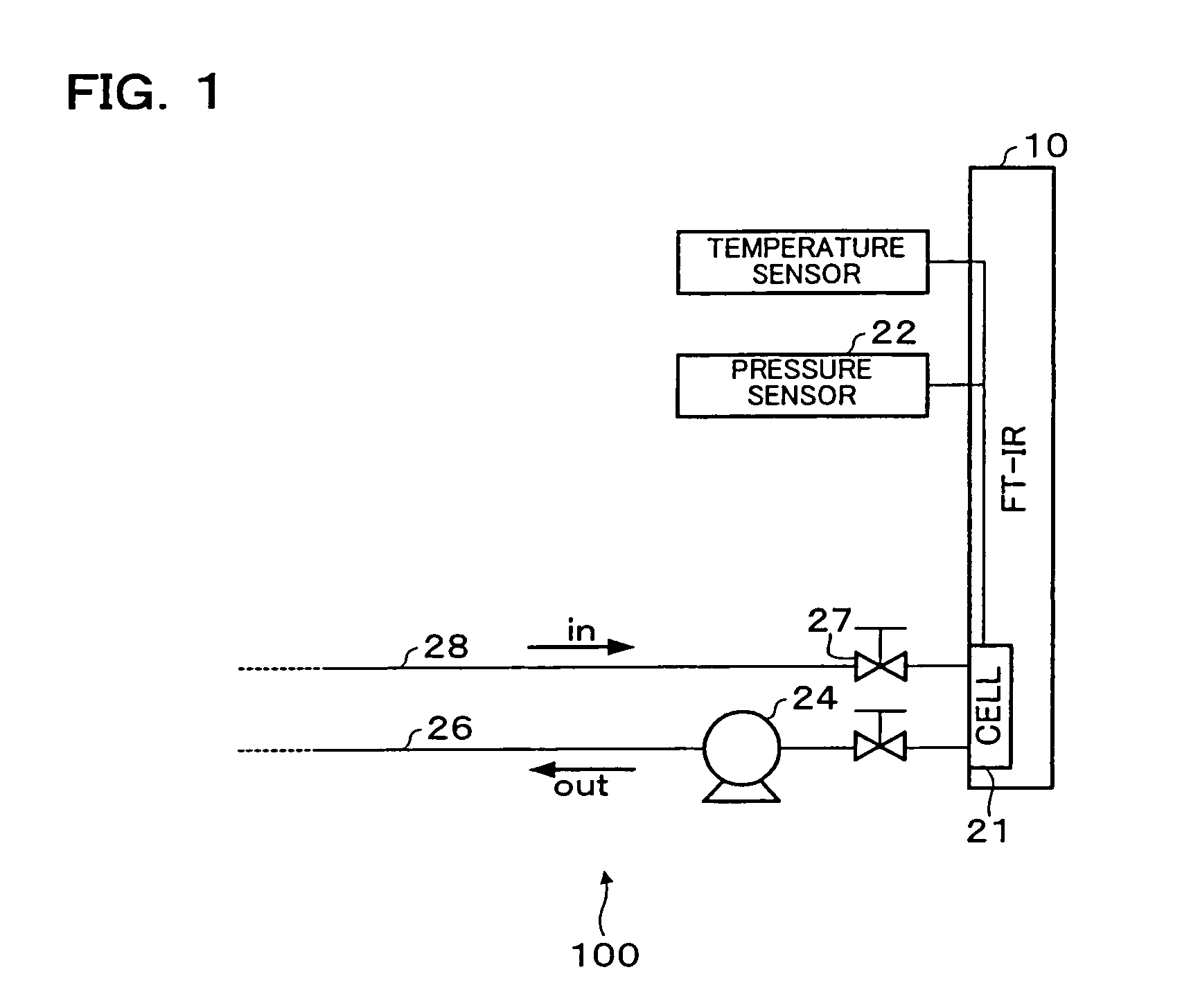
[0119]FIG. 2 schematically shows semiconductor manufacturing equipment 11 connected with the infrared absorption measurement device 100 in the present embodiment. The present embodiment illustrates the case where the infrared absorption measurement device 100 in the first embodiment is used to quantitatively analyze the measurement target component included in the gas discharged from the semiconductor manufacturing equipment 11.
[0120]In the infrared absorption measurement device 100 in the present embodiment, a gas discharged from the semiconductor manufacturing equipment 11 is mixed with nitrogen gas 20 to form a sample gas. The sample gas is introduced into the infrared absorption analysis device 10 through the gas inlet line 28, and infrared absorption of each measurement target component included in the sample gas is measured by using the infrared absorption analysis device 10.
[0121]In the semiconductor manufacturing equipment 11, a semiconductor manufacturin...
third embodiment
3. Third Embodiment
3-1. Infrared Absorption Measurement Device
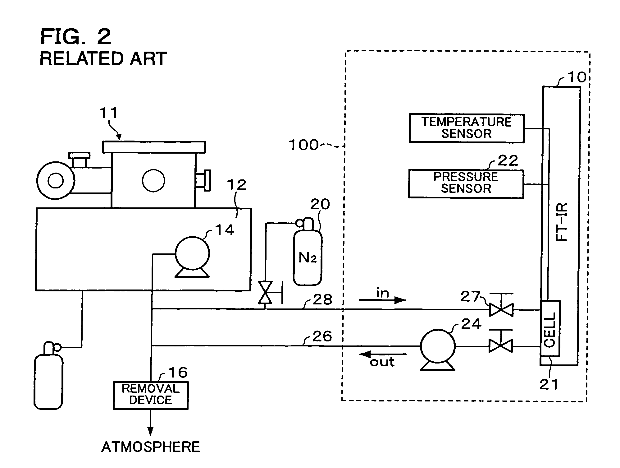
[0133]FIG. 3 schematically shows an infrared absorption measurement device 200 in the present embodiment and the semiconductor manufacturing equipment 11 connected with the infrared absorption measurement device 200. The present embodiment illustrates the case where the infrared absorption measurement device 200 is used to quantitatively analyze the measurement target component included in the gas discharged from the semiconductor manufacturing equipment 11. Specifically, the present embodiment is the same as the second embodiment in that the infrared absorption measurement device is used to quantitatively analyze the measurement target component included in the gas discharged from the semiconductor manufacturing equipment 11.
[0134]The infrared absorption measurement device 200 in the present embodiment has a configuration differing from the configuration of the infrared absorption measurement device 100 in the first embo...
PUM
 Abstract
Description
Claims
Application Information
 - R&D
- Intellectual Property
- Life Sciences
- Materials
- Tech Scout
- Unparalleled Data Quality
- Higher Quality Content
- 60% Fewer Hallucinations
Browse by: Latest US Patents, China's latest patents, Technical Efficacy Thesaurus, Application Domain, Technology Topic, Popular Technical Reports.
© 2025 PatSnap. All rights reserved.Legal|Privacy policy|Modern Slavery Act Transparency Statement|Sitemap|About US| Contact US: help@patsnap.com