Drive method for plasma display panel and plasma display device
a technology of plasma display panel and drive method, which is applied in the direction of color television details, television systems, instruments, etc., can solve the problems of insufficient gradation expression and image quality degradation, and achieve the effect of preventing a luminance reversal without degrading image quality
- Summary
- Abstract
- Description
- Claims
- Application Information
AI Technical Summary
Benefits of technology
Problems solved by technology
Method used
Image
Examples
first embodiment
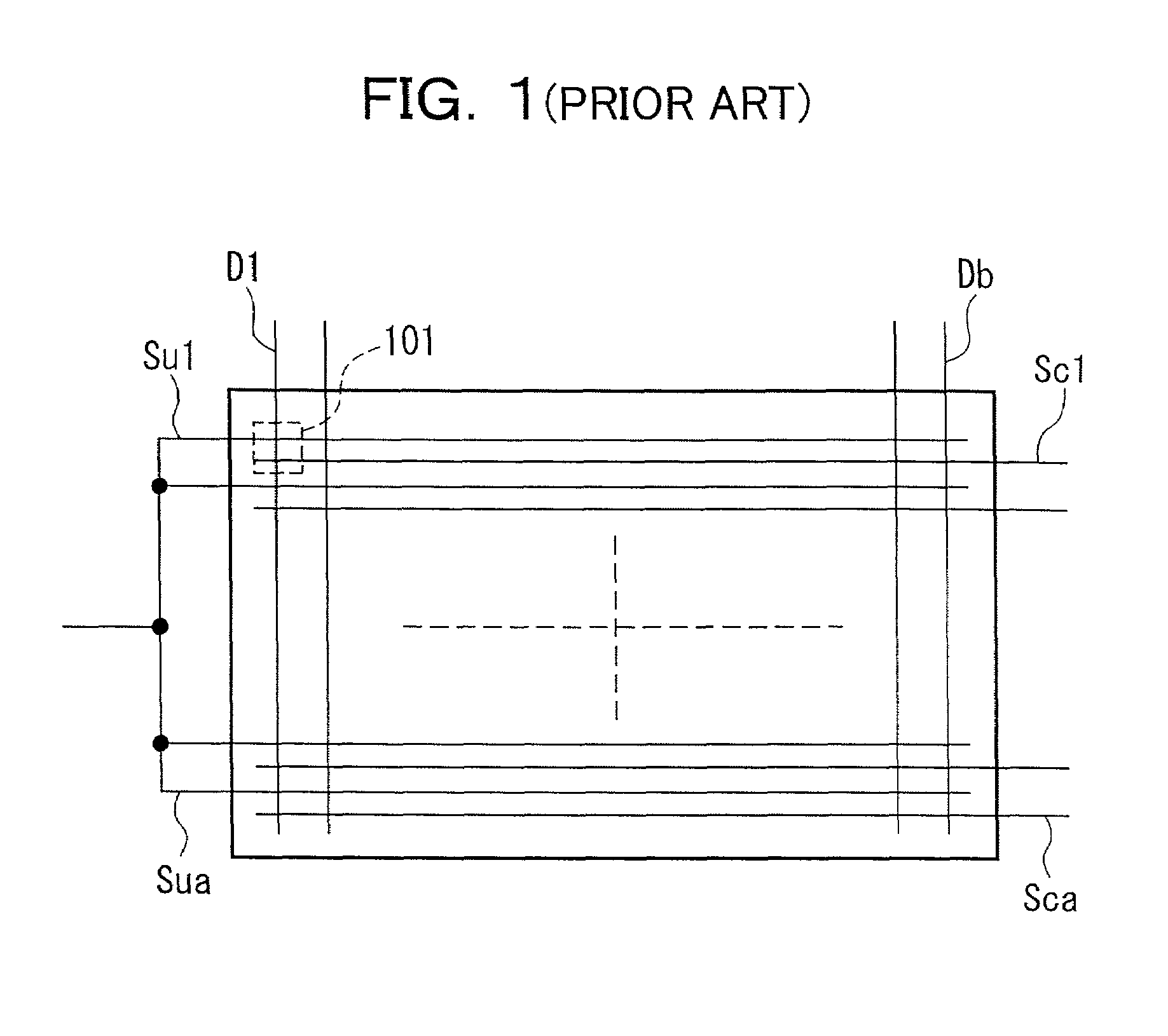
[0037]When the average peak level is low, and there are no subfields with the same sustain cycle numbers, all scan electrodes are scanned, and simultaneously data pulses according to the video signals are impressed on data electrodes in the
[0038]On the other hand, when the average peak level is high, and the sustain cycle numbers are equal in the lowest level subfield SF1 and the second lowest level subfield SF2 while there is a difference in the weight between the lowest level subfield SF1 and the second lowest level subfield SF2 as shown in Table 1, all scan electrodes are scanned, and simultaneously data pulses according to the video signals are impressed only on the odd number data electrodes or the even number data electrodes according to whether the field has an odd number or an even number as shown in FIG. 4 in the subfield SF1. Namely, for the lowest level subfield SF1 of an odd number filed (nth (n: odd number) frame), the data pulses are impressed on the data electrodes ac...
second embodiment
[0046]With the second embodiment, in the lowest subfield SF1, the selectable pixels receiving the data pulses are arranged in a checkerboard pattern, and the selectable state and the unselectable state are switched for all the pixels for every frame as shown in FIG. 7A and FIG. 7B. As a result, the sustain cycle number for the lowest level subfield SF1 virtually becomes 0.5, which is a half of 1, and is a half of the sustain cycle number of the subfield SF2, which is on one upper level. Consequently, because the luminance increases as the gradation level increases, the reversal of the luminance is prevented.
[0047]Because the selectable pixels are arranged as lines in the first embodiment, more or less flickers may occur. On the other hand, because the selectable pixels are arranged in a checkerboard pattern, no flickers occur in the second embodiment.
[0048]The following section describes a third embodiment. FIG. 8 includes drawings showing a relationship between selectable display c...
fourth embodiment
[0058]With the fourth embodiment, the sustain cycle number for the lowest level subfield SF1 virtually becomes 0.25, which is one fourth of 1, and is one fourth of the sustain cycle number of the subfield SF2, which is on one upper level. When the lowest level subfield SF1, the second lowest level subfield SF2, and the third lowest level subfield SF3 have the same sustain cycle number of 1, the following constitution provides a sufficient gradation display without a reversal of the luminance. For the subfield SF3, the sustain cycle number is maintained as 1. For the subfield SF2, any one of the embodiments 1 to 3 is used for virtually reducing the sustain cycle number by half to 0.5. For the subfield SF1, the embodiments 4 is used for virtually reducing the sustain cycle number to 0.25.
[0059]The unit for switching between the selectable state and the unselectable state is not limited to the display cell or the pixel. For example, a block is set per data driver with which the plurali...
PUM
 Abstract
Description
Claims
Application Information
 - R&D
- Intellectual Property
- Life Sciences
- Materials
- Tech Scout
- Unparalleled Data Quality
- Higher Quality Content
- 60% Fewer Hallucinations
Browse by: Latest US Patents, China's latest patents, Technical Efficacy Thesaurus, Application Domain, Technology Topic, Popular Technical Reports.
© 2025 PatSnap. All rights reserved.Legal|Privacy policy|Modern Slavery Act Transparency Statement|Sitemap|About US| Contact US: help@patsnap.com


