Diversity antenna apparatus
- Summary
- Abstract
- Description
- Claims
- Application Information
AI Technical Summary
Benefits of technology
Problems solved by technology
Method used
Image
Examples
first embodiment
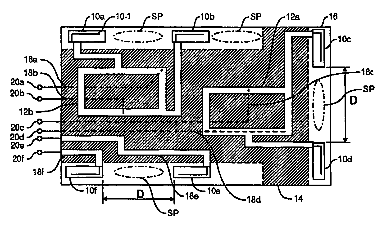
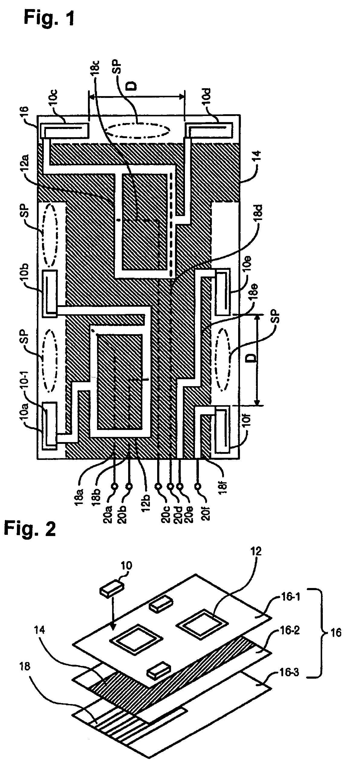
[0047]FIG. 1 is a plane view showing the structure of an antenna substrate in a diversity antenna apparatus according to the present invention. Referring to FIG. 1, the antenna substrate according to this embodiment includes hybrid patterns 12a and 12b, a ground pattern 14, and connecting patterns 18a to 18f that are formed in a printed board 16 comprising at least one layer, for example, three layers. On a top surface of the antenna substrate, a plurality of chip antennas 10a to 10f is mounted. That is, the chip antennas 10a to 10f, i.e., antenna elements, and the ground pattern are disposed substantially on the same plane. Thus, very little space is needed in the height direction.
[0048]Each of the chip antennas 10a to 10f may comprise an element 10-1 formed on a dielectric substrate composed of, for example, a ceramic material, and may be disposed with a certain gap from the ground pattern 14 which inhibits impedance mismatching. The type of the chip antennas 10a to 10f can be any...
second embodiment
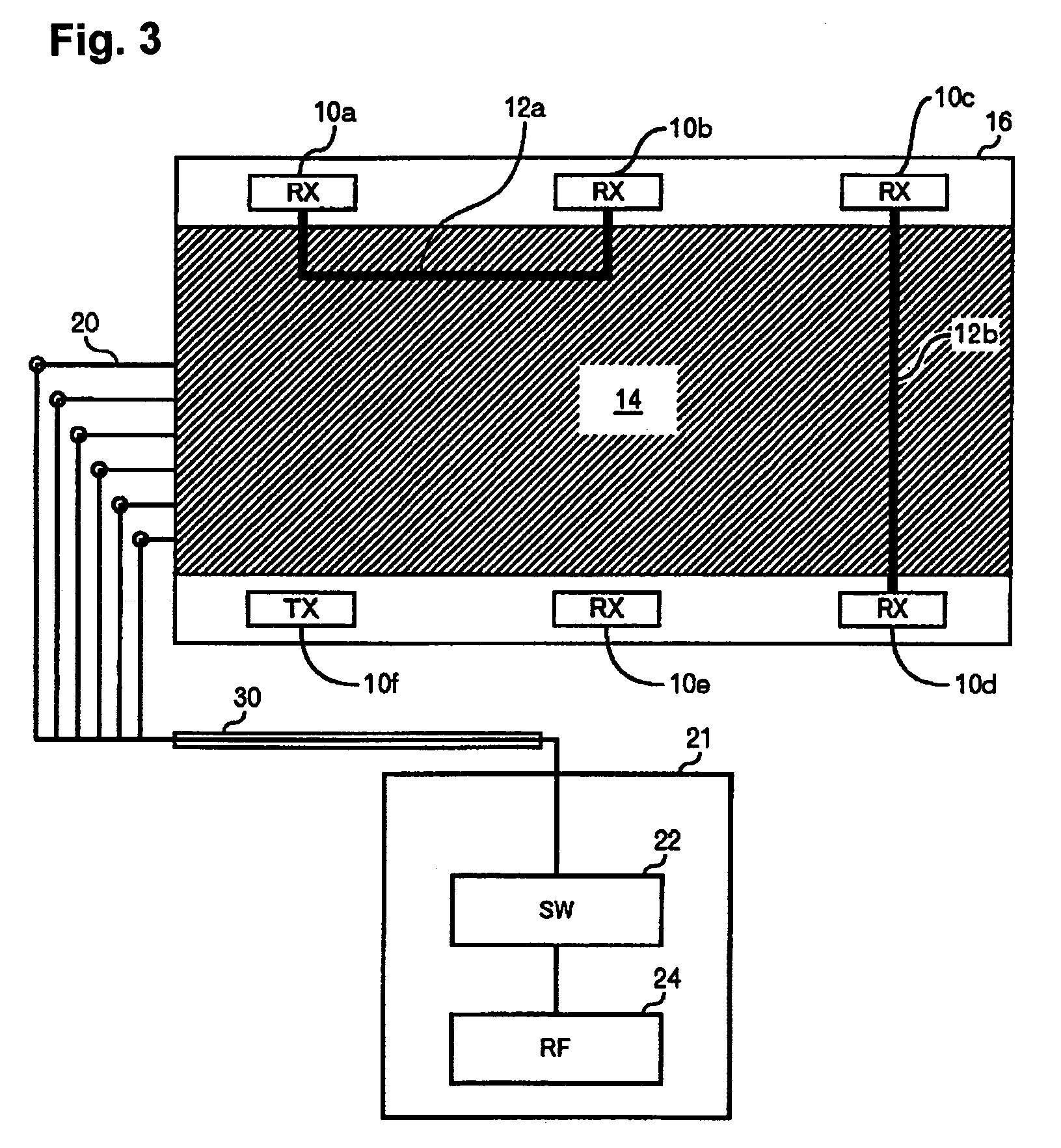
[0075]FIG. 8 shows a modification of the In the modification shown in FIG. 8, receiving antennas 10b to 10f are disposed along the outer edges of the printed board 16 so as to surround a receiving ground pattern 14c that is disposed in a substantially central region of the printed board 16, with a certain gap from the ground pattern 14c. Similarly to the arrangement described earlier, the gap between the receiving chip antenna 10b and the receiving chip antenna 10c and the gap between the receiving chip antenna 10e and the receiving chip antenna 10d are not smaller than λ / 4. The shape of the ground pattern 14c is rectangular in this modification, but the ground pattern 14c may have other shapes. However, preferably, the ground pattern 14c does not cover a region between the receiving chip antennas 10b and 10c, a region between the receiving chip antennas 10f and 10e, or a region between the receiving chip antennas 10e and 10d.
[0076]In the modification shown in FIG. 8, similarly to...
PUM
 Abstract
Description
Claims
Application Information
 - R&D
- Intellectual Property
- Life Sciences
- Materials
- Tech Scout
- Unparalleled Data Quality
- Higher Quality Content
- 60% Fewer Hallucinations
Browse by: Latest US Patents, China's latest patents, Technical Efficacy Thesaurus, Application Domain, Technology Topic, Popular Technical Reports.
© 2025 PatSnap. All rights reserved.Legal|Privacy policy|Modern Slavery Act Transparency Statement|Sitemap|About US| Contact US: help@patsnap.com


