Patterned plasma treatment to improve distribution of underfill material

a plasma treatment and underfill material technology, applied in the direction of semiconductor devices, electrical equipment, semiconductor/solid-state device details, etc., can solve the problems of short between the bumps, the chip may not function properly or at all, and the crack may propagate into the chip itself and/or, so as to increase the capillary force and enhance the distribution of underfill material

Active Publication Date: 2006-05-16
TEXAS INSTR INC
View PDF0 Cites 3 Cited by
  • Summary
  • Abstract
  • Description
  • Claims
  • Application Information

AI Technical Summary

Benefits of technology

[0011]The problems and needs outlined above may be addressed by embodiments of the present invention. A patterned plasma treatment may be provided on the chip and / or the substrate to enhance the distribution of underfill material between the chip and the substrate. The underfill material is typically dispensed after the chip is electrically connected to the substrate. The chip may be electrically connected to the substrate by an array of solder bumps, as one example. The underfill material is draw into a gap between the chip and the substrate by a capillary action. The patterned plasma-treated area formed on the chip and / or on the substrate may cause greater capillary force on the underfill material, as compared to non-plasma-treated areas. Such patterned plasma-treatment area may be designed and laid out to provide for more or better control of the underfill distribution between the chip and substrate while forming a chip package.

Problems solved by technology

A crack may propagate into the chip itself and / or through a solder bump or some other line in the chip or substrate.
This may cause a failure site or an open connection, either of which is highly undesirable and may cause the chip to function improperly or fail to function at all.
Also, if a void happens to be located between two solder bumps, the material from those solder bumps may eventually extrude into the void causing a short between those bumps.
This is also highly undesirable.
As discussed above, such air pockets or voids are highly undesirable.

Method used


Image

  • Patterned plasma treatment to improve distribution of underfill material
  • Patterned plasma treatment to improve distribution of underfill material
  • Patterned plasma treatment to improve distribution of underfill material

Examples


Embodiment Construction

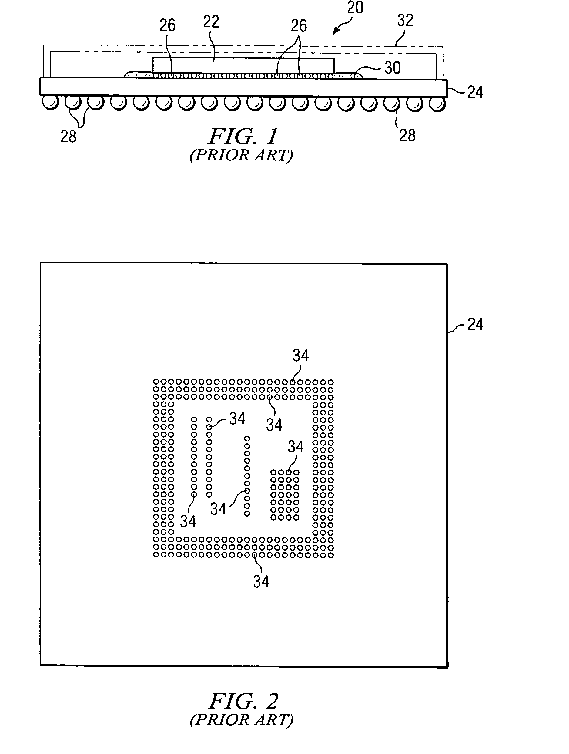
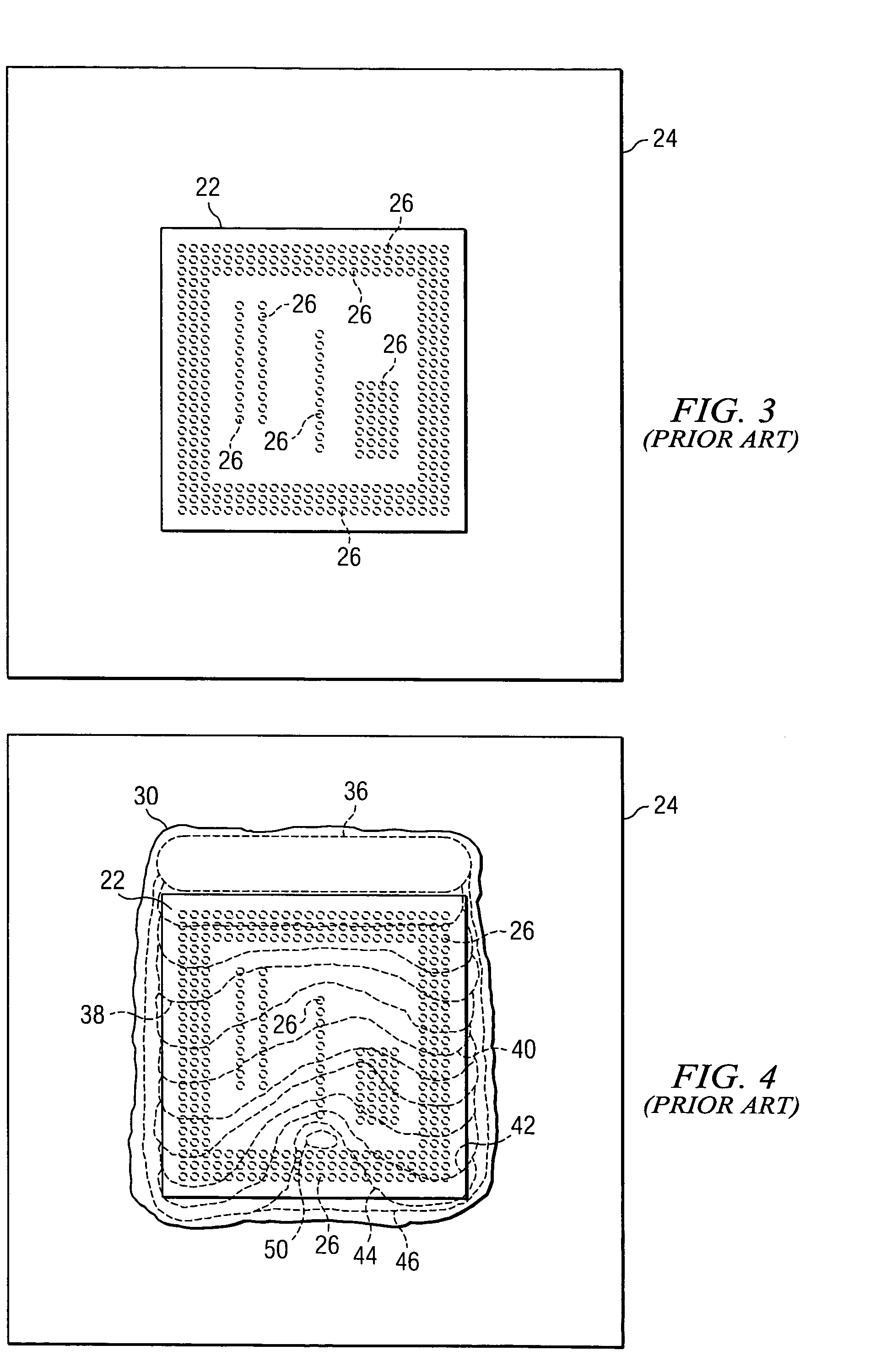
[0032]Referring now to the drawings, wherein like reference numbers are used herein to designate like elements throughout the various views, illustrative embodiments of the present invention are shown and described. The figures are not necessarily drawn to scale, and in some instances the drawings have been exaggerated and / or simplified in places for illustrative purposes only. One of ordinary skill in the art will appreciate the many possible applications and variations of the present invention based on the following illustrative embodiments of the present invention.

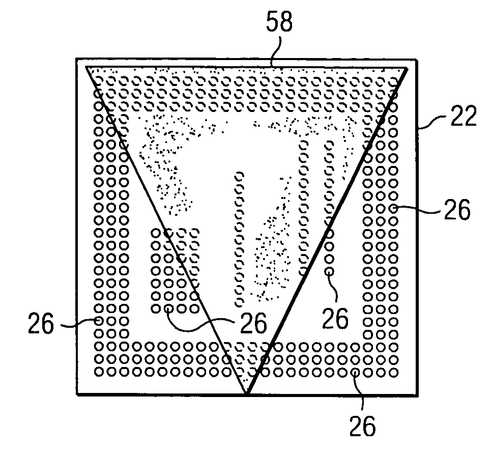
[0033]Plasma treating a surface of the chip 22 and / or the substrate 24 may increase or enhance the flow rate of underfill material 30 between the chip 22 and the substrate 24. Also, such plasma treatment may improve adhesion of the underfill material 30 with the chip 22 and / or substrate 24. The plasma treatment may achieve these benefits in a number of ways. The plasma treatment may roughen the surface by forming pits i...


PUM


Abstract

A patterned plasma treatment may be provided on the chip and / or the substrate to enhance the distribution of underfill material between the chip and the substrate. The underfill material is typically dispensed after the chip is electrically connected to the substrate. The chip may be electrically connected to the substrate by an array of solder bumps, as one example. The underfill material is draw into a gap between the chip and the substrate by a capillary action. The patterned plasma-treated area formed on the chip and / or on the substrate may cause greater capillary force on the underfill material, as compared to non-plasma-treated areas. Such patterned plasma-treatment area may be designed and laid out to provide for more or better control of the underfill distribution between the chip and substrate while forming a chip package.

Description

TECHNICAL FIELD[0001]The present invention generally relates to providing an underfill layer between a chip and a substrate, such as the case where the chip is electrically connected to the substrate by an array of solder bumps located between the chip and the substrate. In one aspect, it relates to a patterned plasma treatment to improve the distribution of the underfill material.BACKGROUND[0002]Integrated circuit devices typically include a semiconductor die or chip that is assembled in a package. A package typically has a substrate portion that the chip is electrically connected to. Usually the substrate is larger than the chip and has a larger array of leads or electrical contact points than that of the chip to allow for ease of assembly of the packaged chip onto a circuit board. One such package configuration is a flip-chip package.[0003]An example of a conventional flip-chip package 20 is shown in FIG. 1. In this example, the chip 22 is electrically connected to the substrate ...

Claims


Application Information

Patent Timeline
Patent Type & Authority Patents(United States)
IPC IPC(8): H01L29/40H01L21/56H01L23/22
CPCH01L21/563H01L24/27H01L2224/73203H01L2224/16225H01L2924/01029H01L2224/73204H01L2924/15311H01L2224/32225H01L2924/00H01L2924/3512H01L2924/14
Inventor ODEGARD, CHARLES ANTHONYYUNUS, MOHAMMADARABE, FERDINAND BORROMEO
Owner TEXAS INSTR INC
Why Eureka
Try Eureka