Optical deflection device and optical deflection method that control occurrence of alignment defect
a technology alignment defect, which is applied in the direction of instruments, non-linear optics, optics, etc., can solve the problems of difficult to achieve small optical deflection device, limited use of optical deflection device, and difficulty in making the speed of response faster to the order of sub-milliseconds
- Summary
- Abstract
- Description
- Claims
- Application Information
AI Technical Summary
Benefits of technology
Problems solved by technology
Method used
Image
Examples
examples
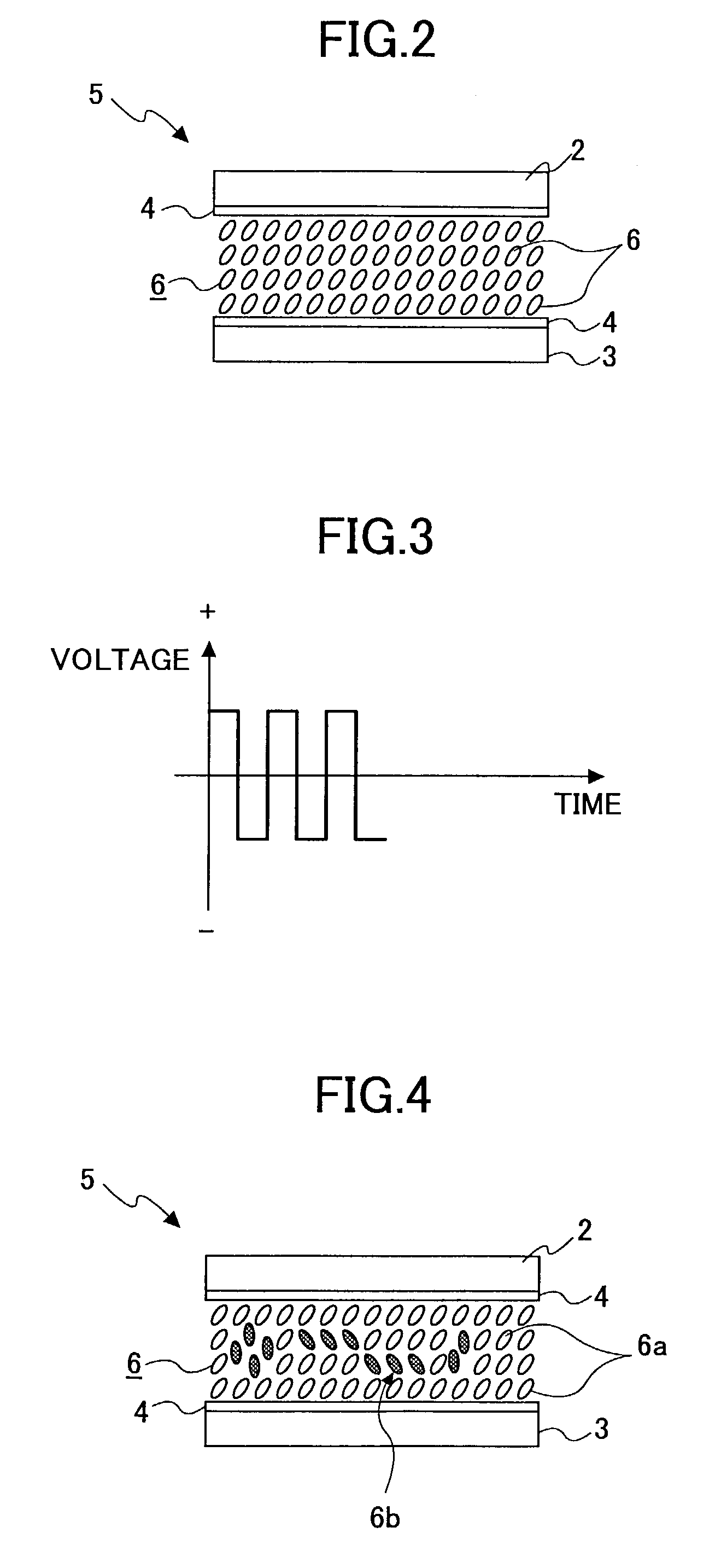
[0260]A description will be given of examples of the present invention. In the examples, three kinds of optical deflection elements A, B and C are prepared. As will be described in Examples 1 through 4 and Comparative Examples 1 and 2, the evaluations of variation in performance through repeated use are made by varying the application method of a voltage to the optical deflection elements A, B and C.
[0261]First, a surface of a glass board (the boards 2 and 3), having the size of 3 cm×4 cm with the thickness of 1 mm, was treated with a perpendicular orientation film JALS2021-R2 (manufactured by JSR Corporation) so as to form a perpendicular orientation film (the orientation film 4) on one side of the glass board. Two of such glass boards were bonded together with the perpendicular orientation films inside while interposing therebetween two aluminum electrode sheets (the electrodes 7a and 7b) as spacers, each of the aluminum electrode sheets having the thickness of 50 μm, the width of...
example 1
[0268]In Example 1, using the optical deflection element A, the ac voltage of ±200 V and 100 Hz, which was similar to the pixel shift driving, was applied for 40 minutes in a similar manner. Thereafter, an ac voltage of ±100 V and 1 kHz was applied for one minute before stopping the optical deflection operation. Then, the orientation state of the liquid crystal layer thereafter was observed.
[0269]As a result, in the Example 1, white turbidity was not developed in the vicinities of the electrodes. Although a similar optical deflection operation was repeated thereafter, white turbidity was not developed.
example 2
[0270]In Example 2, using the optical deflection element A, the ac voltage of ±200 V and 100 Hz, which was similar to the pixel shift driving, was applied for 40 minutes in a similar manner. Then, a pulsed dc voltage of +200 V is applied ten times in one minute and stopped. Then, the orientation state of the liquid crystal thereafter was observed.
[0271]Consequently, in Example 2, white turbidity was not developed in the vicinities of the electrodes. Thereafter, though the similar optical deflection operation was repeated, white turbidity was not developed.
PUM
| Property | Measurement | Unit |
|---|---|---|
| driving frequency | aaaaa | aaaaa |
| deflection frequency | aaaaa | aaaaa |
| frequency | aaaaa | aaaaa |
Abstract
Description
Claims
Application Information
 - R&D
- Intellectual Property
- Life Sciences
- Materials
- Tech Scout
- Unparalleled Data Quality
- Higher Quality Content
- 60% Fewer Hallucinations
Browse by: Latest US Patents, China's latest patents, Technical Efficacy Thesaurus, Application Domain, Technology Topic, Popular Technical Reports.
© 2025 PatSnap. All rights reserved.Legal|Privacy policy|Modern Slavery Act Transparency Statement|Sitemap|About US| Contact US: help@patsnap.com


