Full-color organic display having improved blue emission
a full-color organic display and blue emission technology, applied in the direction of discharge tube luminescnet screens, discharge tube/lamp details, electric discharge lamps, etc., can solve the problem of limited life of full-color organic displays, achieve the effect of increasing luminous efficiency, reducing surface emission areas, and increasing lifetim
- Summary
- Abstract
- Description
- Claims
- Application Information
AI Technical Summary
Benefits of technology
Problems solved by technology
Method used
Image
Examples
example 1
Comparative
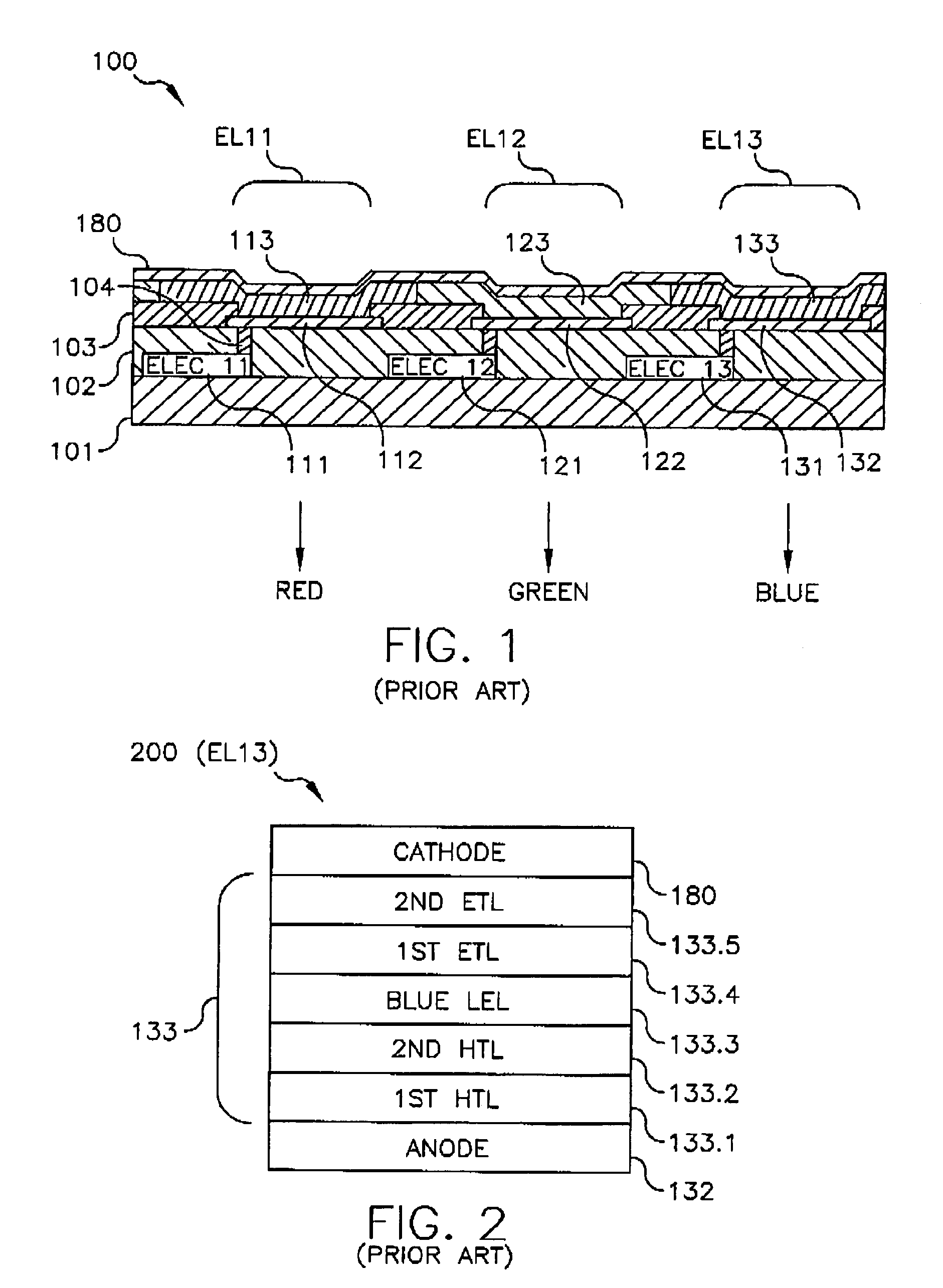
[0124]The preparation of a conventional blue EL subpixel is as follows: A ˜1.1 mm thick glass substrate coated with a transparent ITO conductive layer was cleaned and dried using a commercial glass scrubber tool. The thickness of ITO is about 42 nm and the sheet resistance of the ITO is about 68 Ω / square. The ITO surface was subsequently treated with oxidative plasma to condition the surface as an anode. A layer of CFx, 1 nm thick, was deposited on the clean ITO surface as the HIL by decomposing CHF3 gas in an RF plasma treatment chamber. The substrate was then transferred into a vacuum deposition chamber (TROVATO MFG. INC) for deposition of all other layers on top of the substrate. The following layers were deposited in the following sequence by evaporation from a heated boat under a vacuum of approximately 10−6 Torr:[0125]1. EL unit:[0126](1) a first HTL, about 70 nm thick, consisting of m-TDATA doped with 3.0 vol. % F4-TCNQ;[0127](2) a second HTL, 10 nm thick, consisti...
example 2
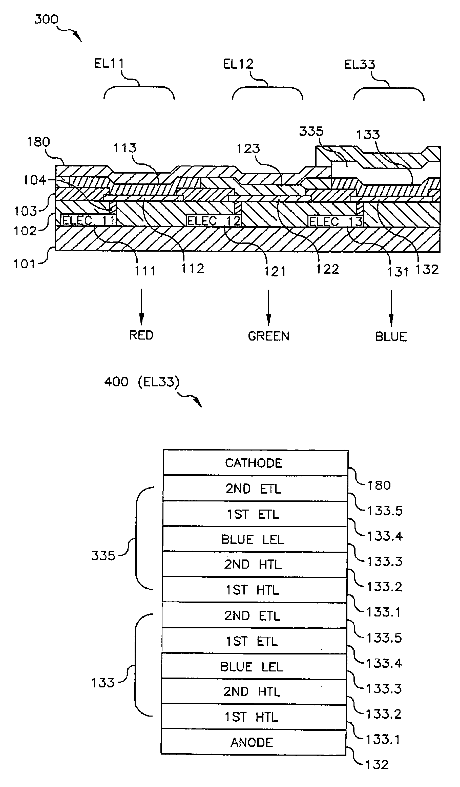
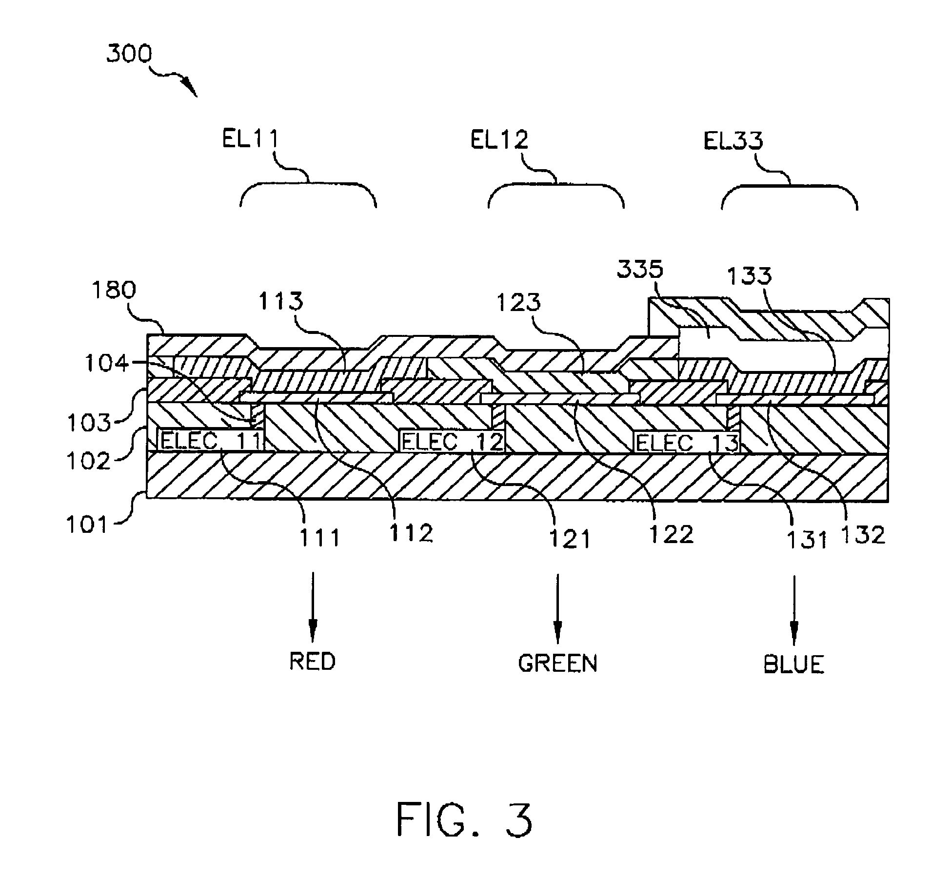
[0133]A blue EL subpixel was constructed in the manner described in Example 1, and the deposited layer structure is:[0134]1. 1st EL unit:[0135](1) a first HTL, about 70 nm thick, consisting of m-TDATA doped with 3.0 vol. % F4-TCNQ;[0136](2) a second HTL, 10 nm thick, consisting of NPB;[0137](3) a LEL, 20 nm thick, consisting of TBADN doped with 1.5 vol. % TBP;[0138](4) a first ETL, 10 nm thick, consisting of Bphen; and[0139](5) a second ETL, 25 nm thick, consisting of Bphen doped with 1.2 vol. % Li.[0140]2. 2nd EL unit:[0141](1) a first HTL, about 55 nm thick, consisting of m-TDATA doped with 3.0 vol. % F4-TCNQ;[0142](2) a second HTL, 10 nm thick, consisting of NPB;[0143](3) a LEL, 20 nm thick, consisting of TBADN doped with 1.5 vol. % TBP;[0144](4) a first ETL, 10 nm thick, consisting of Bphen; and[0145](5) a second ETL, 25 nm thick, consisting of Bphen doped with 1.2 vol. % Li.[0146]3. Cathode: approximately 330 nm thick, consisting of MgAg.
[0147]The EL performance of the device w...
PUM
 Abstract
Description
Claims
Application Information
 - R&D Engineer
- R&D Manager
- IP Professional
- Industry Leading Data Capabilities
- Powerful AI technology
- Patent DNA Extraction
Browse by: Latest US Patents, China's latest patents, Technical Efficacy Thesaurus, Application Domain, Technology Topic, Popular Technical Reports.
© 2024 PatSnap. All rights reserved.Legal|Privacy policy|Modern Slavery Act Transparency Statement|Sitemap|About US| Contact US: help@patsnap.com


