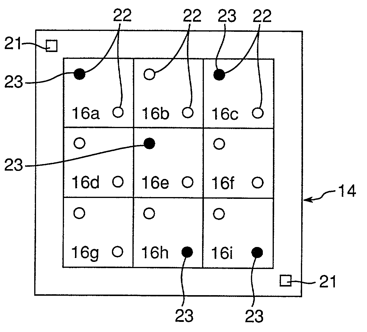
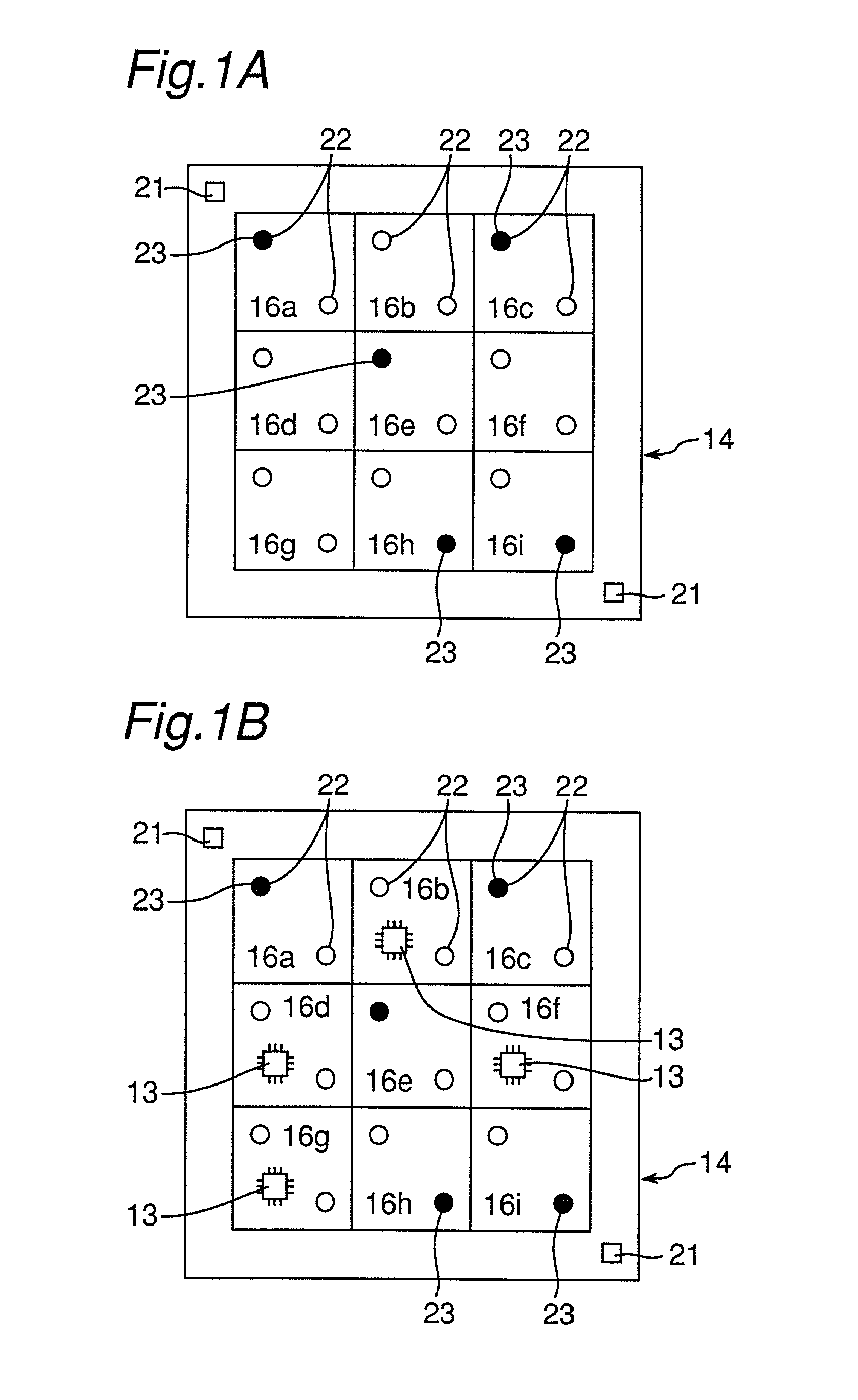
[0018]The present invention provides a method of mounting a component, which comprises steps of: recognizing a bad mark which is indicated on a circuit-formed substrate when each of at least one individual substrate provided by sectioning the circuit-formed substrate includes a defective individual substrate, and recognizing an individual substrate mark which is provided on the circuit-formed substrate so as to recognize a position and an inclination of each of at least one individual substrate as above; and mounting a component onto the circuit-formed substrate, aiming at an individual substrate having no bad mark indicated; and the invention is characterized in that the bad mark is indicated on the individual substrate mark. This method is effective to improve efficiency of a recognition operation by using the individual substrate mark also as the bad mark.
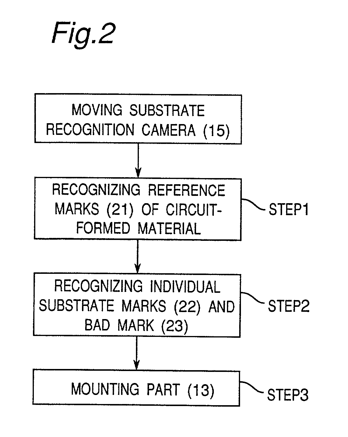
[0019]Another aspect of the present invention provides a method for mounting a component, which comprises steps of: recognizing a condition of a sucked component which is fed by a component-feeding device, sucked and removed therefrom; recognizing a condition of a secured circuit-formed substrate which is carried, regulated and secured; recognizing a position and an inclination of at least one individual substrate provided by sectioning the circuit-formed substrate; calculating correction amounts for a position and inclination of the component, which is to be mounted, based on a result of recognition of the component-sucking condition, a result of recognition of the circuit-formed substrate-securing condition, and a result of recognition of the position and inclination of the individual substrate; and making necessary correction on the component based on the result of the above calculation, and mounting the component at a predetermined position on the individual substrate; and the invention is characterized in that a mark which is provided on the individual substrate so as to recognize the position and inclination of the individual substrate is used also as a bad mark for discriminating a defective individual substrate. This method is effective to reduce a number of the recognition operations performed by the substrate-recognition camera, by using the individual substrate mark also as the bad mark.
[0021]Another aspect of the present invention provides a method for mounting a component, which comprises steps of: recognizing a condition of a sucked component which is fed from a component-feeding unit, sucked and removed therefrom; recognizing a condition of a secured circuit-formed substrate which is carried, regulated and secured; recognizing a position and inclination of at least one individual substrate provided by sectioning the circuit-formed substrate; calculating correction amounts for a position and inclination of the component, which is to be mounted, based on results of the recognition of the component-sucking condition, the circuit-formed substrate-securing condition, and the position and inclination of the individual substrate; and making necessary correction of the component based on the result of the above calculation, and mounting the component at a predetermined position on the individual substrate, and the invention is characterized in that a position at which a substrate-recognition camera should recognize the position and inclination of the individual substrate is controlled based on the result of the recognition of the circuit-formed substrate-securing condition. This method is effective to avoid occurrence of a recognition error by utilizing the inclination of the circuit-formed substrate and the
dislocation of the position thereof for the recognition operation of the individual substrate.
[0022]Another aspect of the present invention provides a method for mounting a component, which comprises steps of: recognizing a condition of a sucked component which is fed from a component-feeding unit, sucked and removed therefrom; recognizing a condition of a secured circuit-formed substrate which is carried, regulated and secured; recognizing a position and inclination of at least one individual substrate provided by sectioning the circuit-formed substrate; calculating correction amounts for a position and inclination of the component, which is to be mounted, based on results of recognition of the component-sucking condition, the circuit-formed substrate-securing condition, and the position and inclination of the individual substrate; and making necessary correction of the component based on the result of the above calculation, and mounting the component at a predetermined position on the individual substrate; and the invention is characterized in that, when a portion or a whole of a mark provided on the circuit-formed substrate so as to recognize the circuit-formed substrate-securing condition, or a mark provided on the individual substrate so as to recognize the condition of the individual substrate, is not included within a visual field of a substrate-recognition camera for recognizing these marks, a position of the mark is detected and the mark is again recognized. This method is effective to improve yield of non-defectives by detecting the position of the mark and again recognizing the same mark, even if a recognition error occurs.
[0025]Another aspect of the present invention provides a component-mounting apparatus which comprises: a component-feeding unit for feeding a component to be mounted; a mounting head for removing the component from the component-feeding unit and mounting it on a circuit-formed substrate; a component-recognition camera for recognizing a condition of the component when held by the mounting head; an X-Y
robot for carrying the mounting head to a predetermined position; a circuit-formed substrate-securing device for carrying and securing the circuit-formed substrate; a substrate-recognition camera for recognizing a condition of the secured circuit-formed substrate; and a
control unit for controlling overall operations of the apparatus. With the above construction, the substrate-recognition camera recognizes an individual substrate mark which is provided on each of at least one individual substrate provided by sectioning the circuit-formed substrate so as to recognize a position and inclination of the individual substrate; correction amounts for the position and inclination of the component to be mounted are calculated based on a result of this recognition of the individual substrate mark, a result of recognition of the component-holding condition performed by the component-recognition camera, and a result of the recognition of the circuit-formed substrate-securing condition performed by the substrate-recognition camera so as to make necessary correction of the component; and the mounting head is carried by the X-Y
robot so as to
mount the component at a predetermined position on the individual substrate; and the invention is characterized in that a bad mark to be indicated when the circuit-formed substrate includes a defective individual substrate is put on an individual substrate mark of the defective individual substrate so that the substrate-recognition camera can recognize the bad mark at the same time when recognizing the individual substrate mark. Use of this apparatus is effective to improve efficiency of a recognition operation by using the individual substrate mark also as the bad mark.
[0026]Another aspect of the present invention provides a component-mounting apparatus which comprises: a component-feeding unit for feeding a component to be mounted; a mounting head for removing the component from the component-feeding unit and mounting it on a circuit-formed substrate; a component-recognition camera for recognizing a condition of the component when held by the mounting head; an X-Y robot for carrying the mounting head to a predetermined position; a circuit-formed substrate-securing device for carrying and securing the circuit-formed substrate; a substrate-recognition camera for recording and recognizing a condition of the secured circuit-formed substrate; and a
control unit for controlling overall operations of the apparatus. With the above construction, the substrate-recognition camera recognizes an individual substrate mark which is provided on each of at least one individual substrate provided by sectioning the circuit-formed substrate so as to recognize a position and inclination of the individual substrate; correction amounts for a position and inclination of the component to be mounted are calculated based on a result of the recognition of the individual substrate mark, a result of recognition of the component-holding condition by the component-recognition camera, and a result of recognition of the circuit-formed substrate-securing condition by the substrate-recognition camera so as to make necessary correction of the component; and the mounting head is carried by the X-Y robot so as to
mount the component at a predetermined position on the individual substrate; and the invention is characterized in that a position at which the substrate-recognition camera should recognize the individual substrate mark is controlled based on the result of the recognition of the circuit-formed substrate-securing condition. This apparatus makes it possible to avoid such a situation that the individual substrate mark is not recognized at all, as much as possible, by controlling a position of the substrate-recognition camera based on the result of the recognition of the position and inclination of the circuit-formed substrate.


