
Digital film grain

a digital film and grain technology, applied in the field of digital film grains, can solve the problems of reducing degrading the spatial resolution of the images it can convey, and increasing the thickness of silver film, so as to improve the spatial resolution and improve the imaging resolution

Active Publication Date: 2006-03-21
CARESTREAM HEALTH INC
View PDF57 Cites 44 Cited by
  • Summary
  • Abstract
  • Description
  • Claims
  • Application Information

AI Technical Summary

Benefits of technology

[0007]In one embodiment, a miniature signal sensor with a radio frequency transponder is placed in a capillary or well, along with material enhancing the signal, such as x-ray phosphor. Material between the capillaries or forming the walls of the capillaries reduces or prevents the signal generated in each capillary from generating a response in any other capillary. The walls of the capillaries can be reflective for the visible light or for electrons emitted by the phosphor upon absorbing an x-ray in order to reduce loss of signal.
[0010]A flexible substrate may be used for some applications; for example, conforming to a patient for comfort and for improved imaging resolution. The spatial density of sensors may be uniform in order to avoid clumping of response in parts of the image and to maintain predetermined sensitivity to a range of spatial frequencies. The spatial resolution can be improved by preventing spreading of the response to stimulus at one location beyond the diameter of the capillary to other sensors.

Problems solved by technology

Increasing the film's thickness of silver increases its cost and degrades the spatial resolution of the images it can convey.
These phosphor screens are typically brittle slabs of refractive material, susceptible to breakage if dropped or bent.
The mechanical inflexibility of the phosphor screen prevents conforming the screen-film combination to the patient, impairing comfort and image resolution.
The crystalline semiconductive substrate must extend over an area wider than the largest object intended to be imaged, since only one-to-one imaging is typically performed because imaging lenses are not commercially practical for x-rays now.
A crystalline or glass substrate extending more than several centimeters in two dimensions but thinner than a centimeter in its third dimension is expensive, structurally inflexible, and breakable.

Method used


Image

  • Digital film grain
  • Digital film grain
  • Digital film grain

Examples


Embodiment Construction

[0019]The present invention will be directed in particular to elements forming part of, or in cooperation more directly with, the apparatus in accordance with the present invention. It is to be understood that elements not specifically shown or described may take various forms well known to those skilled in the art.

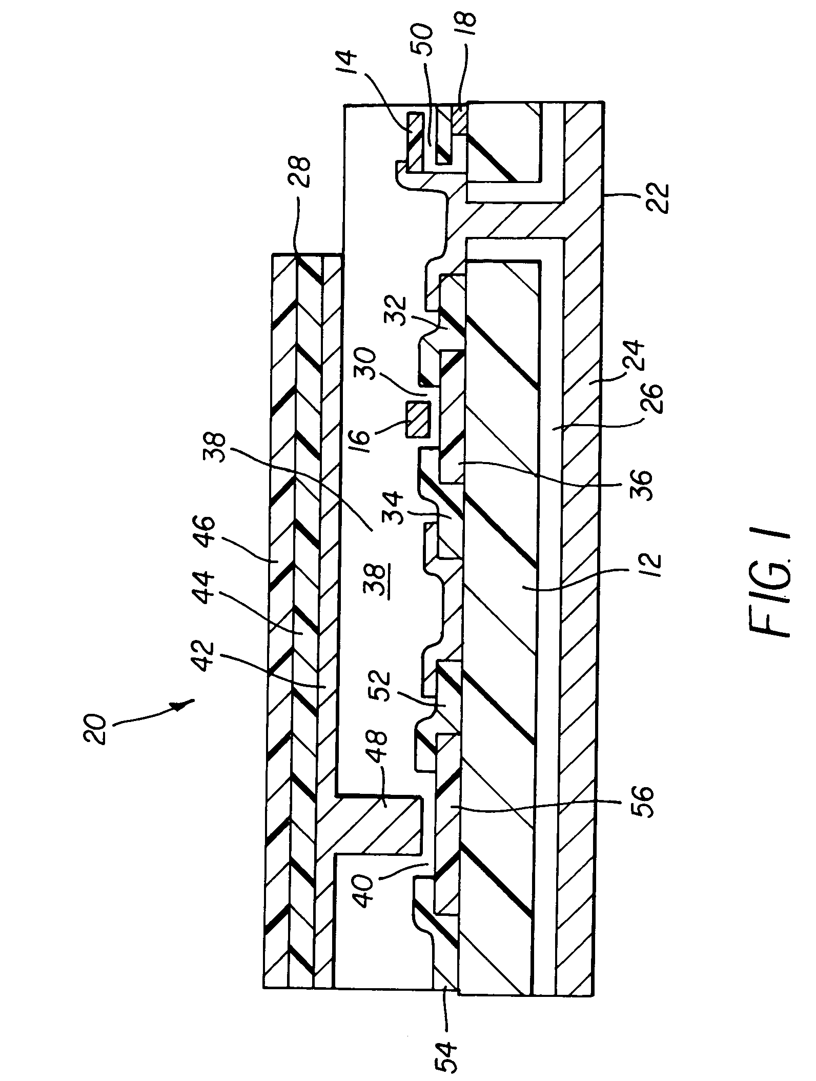
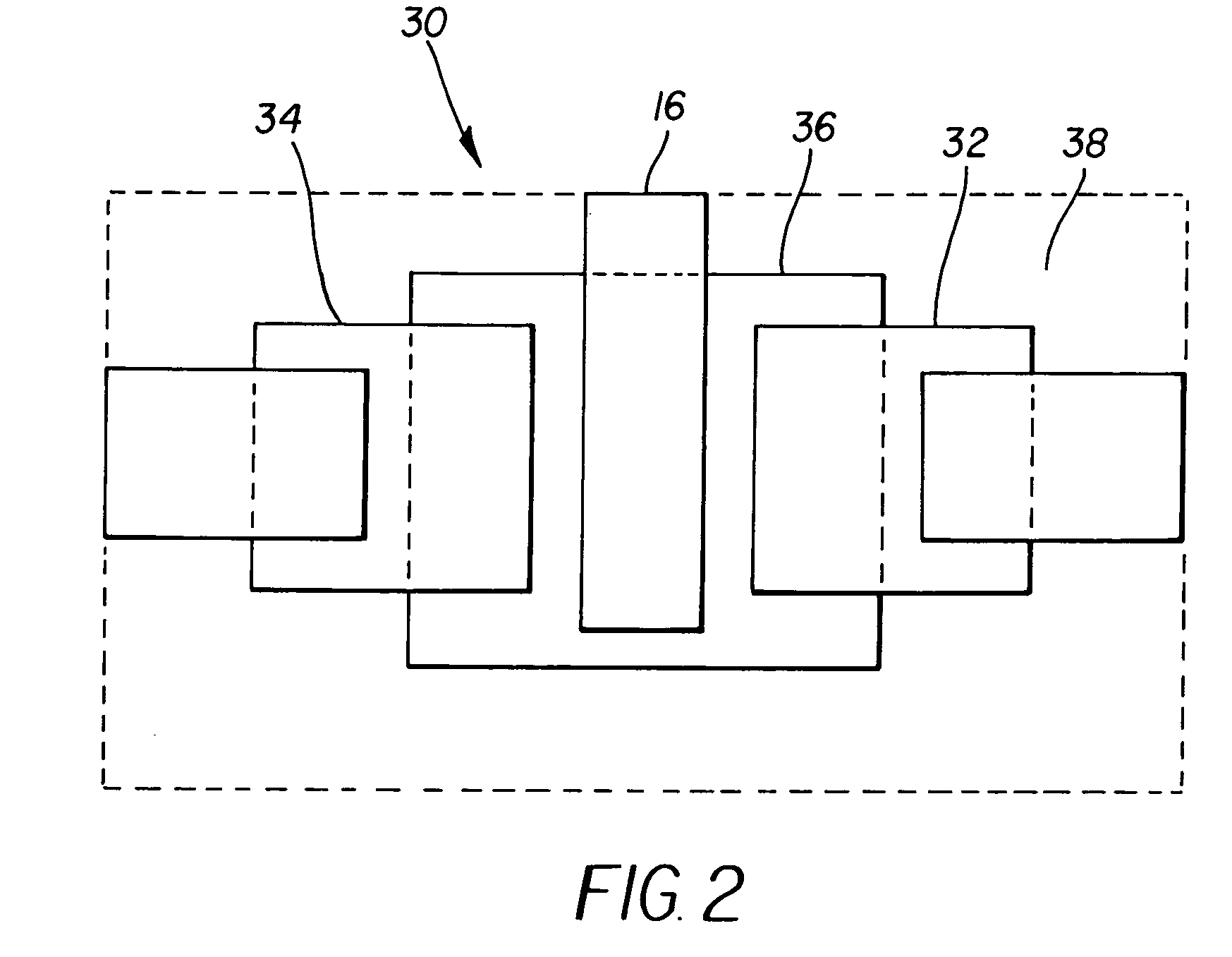
[0020]Referring now to FIG. 1, a p-type layer 36 is deposited on the surface of the crystalline silicon substrate 12 to constitute the central semiconductor of a field-effect transistor 30. Two patches of n-type layer of amorphous silicon are deposited on the surface of the crystalline silicon substrate 12 overlapping p-type layer 36 and fashioned into source 32 and drain 34 of a field-effect transistor 30 shown in FIG. 2. An insulating layer 38 coats p-type layer 36 and at least part of source 32 and drain 34. A gate electrode 16 is fashioned of metal over the p-type layer 36, but separated from electrical contact with that p-type layer 36 by insulator 38, to complete fa...


PUM


Abstract

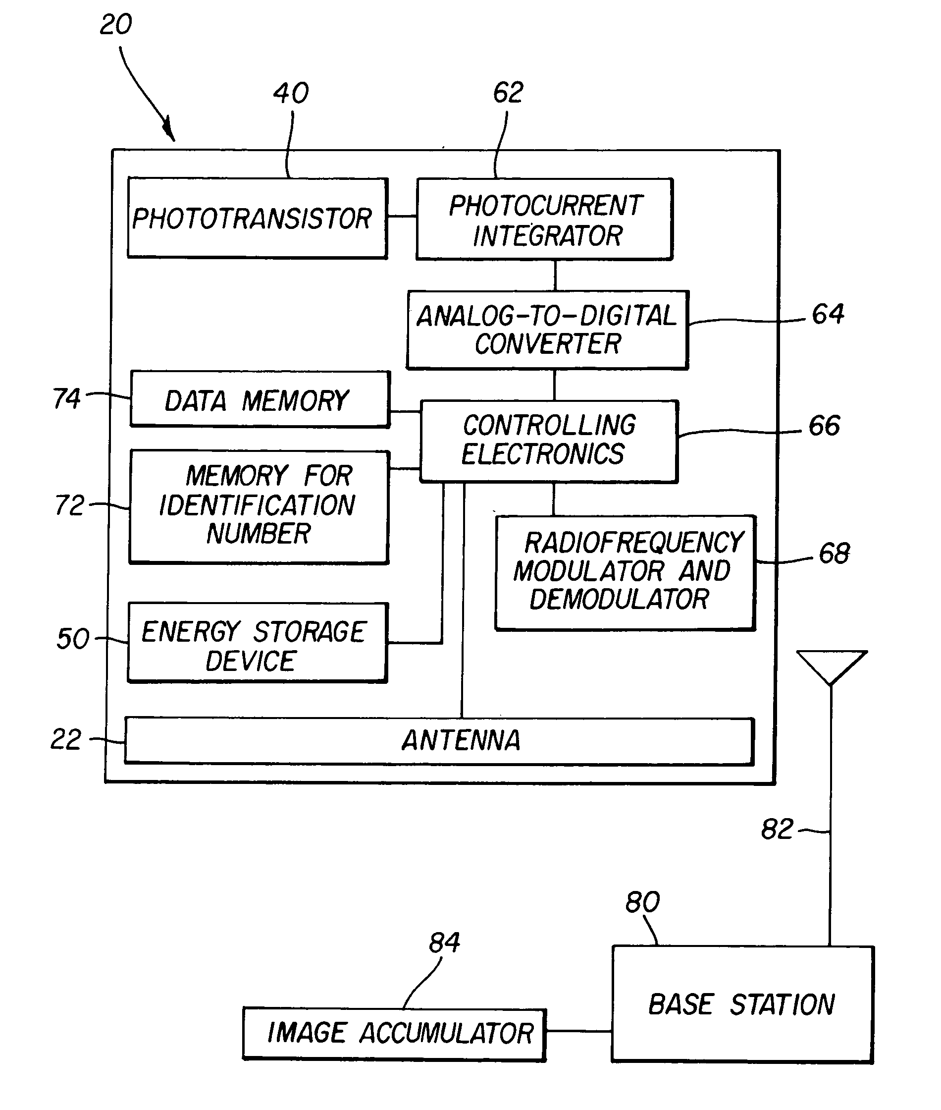
A digital film grain (20) comprises a phototransistor (40) which produces an electrical signal having a strength which is related to an input radiation flux. A transponder receives commands and power from a base station (80) and transmits information quantifying the radiation observed by that digital film grain. An image accumulator (84) connected to the base station (80) assembles an image from the profile of radiation reported by a distribution of digital film grains correlated to the locations of those grains.

Description

FIELD OF THE INVENTION[0001]This invention relates in general to photodetector arrays for acquiring images and in particular to digital film grains.BACKGROUND OF THE INVENTION[0002]X-ray imaging can be performed with silver halide film to detect the x-rays directly or to detect electrons dislodged from an atom in the film by absorption of an x-ray. Each silver halide grain is too thin to absorb an appreciable fraction of the incident x-rays, so that silver halide film exhibits much less sensitivity to x-rays than to visible light. Increasing the film's thickness of silver increases its cost and degrades the spatial resolution of the images it can convey. A screen-film combination interposes a phosphor screen to convert each absorbed x-ray into a burst of visible photons, enhancing the response of the silver halide film. These phosphor screens are typically brittle slabs of refractive material, susceptible to breakage if dropped or bent. The mechanical inflexibility of the phosphor s...

Claims


Application Information

Patent Timeline
Patent Type & Authority Patents(United States)
IPC IPC(8): G01T1/24G01T1/20G01T1/29
CPCH04N5/335G01T1/2928H04N25/00
Inventor HAAS, DANIEL D.MOORE, WILLIAM E.TREDWELL, TIMOTHY J.
Owner CARESTREAM HEALTH INC
Learn More