Semiconductor device and method of manufacturing thereof

a semiconductor device and semiconductor technology, applied in semiconductor devices, diodes, electrical devices, etc., can solve the problem of inability to improve the withstand voltage, and achieve the effect of improving the withstand voltage of the semiconductor device and reducing the flow of reverse recovery curren

Inactive Publication Date: 2005-12-27
MITSUBISHI ELECTRIC CORP
View PDF15 Cites 42 Cited by
  • Summary
  • Abstract
  • Description
  • Claims
  • Application Information

AI Technical Summary

Benefits of technology

[0029]A depletion layer extends from an interface between the impurity region and the semiconductor substrate toward the semiconductor substrate in the reverse bias state in which another prescribed potential is applied to the first electrode layer and the semiconductor substrate respectively. At this time, at a region adjacent to the Schottky junction, the electric field is eased since depletion layers extending from adjacent impurity regions are connected with each other. The depletion layer extends deeper in the semiconductor substrate since each impurity region is formed deeper than the trench portion. Therefore, the distance from the first electrode layer to the edge of the depletion layer increases. The withstand voltage of a semiconductor substrate in the reverse bias state is thus improved.
[0055]In this case, the first electrode layer is in ohmic contact with the impurity region only at the first main surface. Accordingly, an area of a portion in which the first electrode layer and the impurity region are in ohmic contact with each other is reduced. Further, an amount of minority carriers injected from the impurity region into the semiconductor substrate and stored therein in the forward bias state is reduced. As a result, a semiconductor device in which the reverse recovery current is further reduced can be obtained.

Problems solved by technology

This current is especially referred to as reverse recovery current which flows into a semiconductor device such as the IGBT, resulting in the loss.
The withstand voltage is about 100V at most, and improvement of the withstand voltage is impossible.

Method used


Image

  • Semiconductor device and method of manufacturing thereof
  • Semiconductor device and method of manufacturing thereof
  • Semiconductor device and method of manufacturing thereof

Examples


first embodiment

[0081

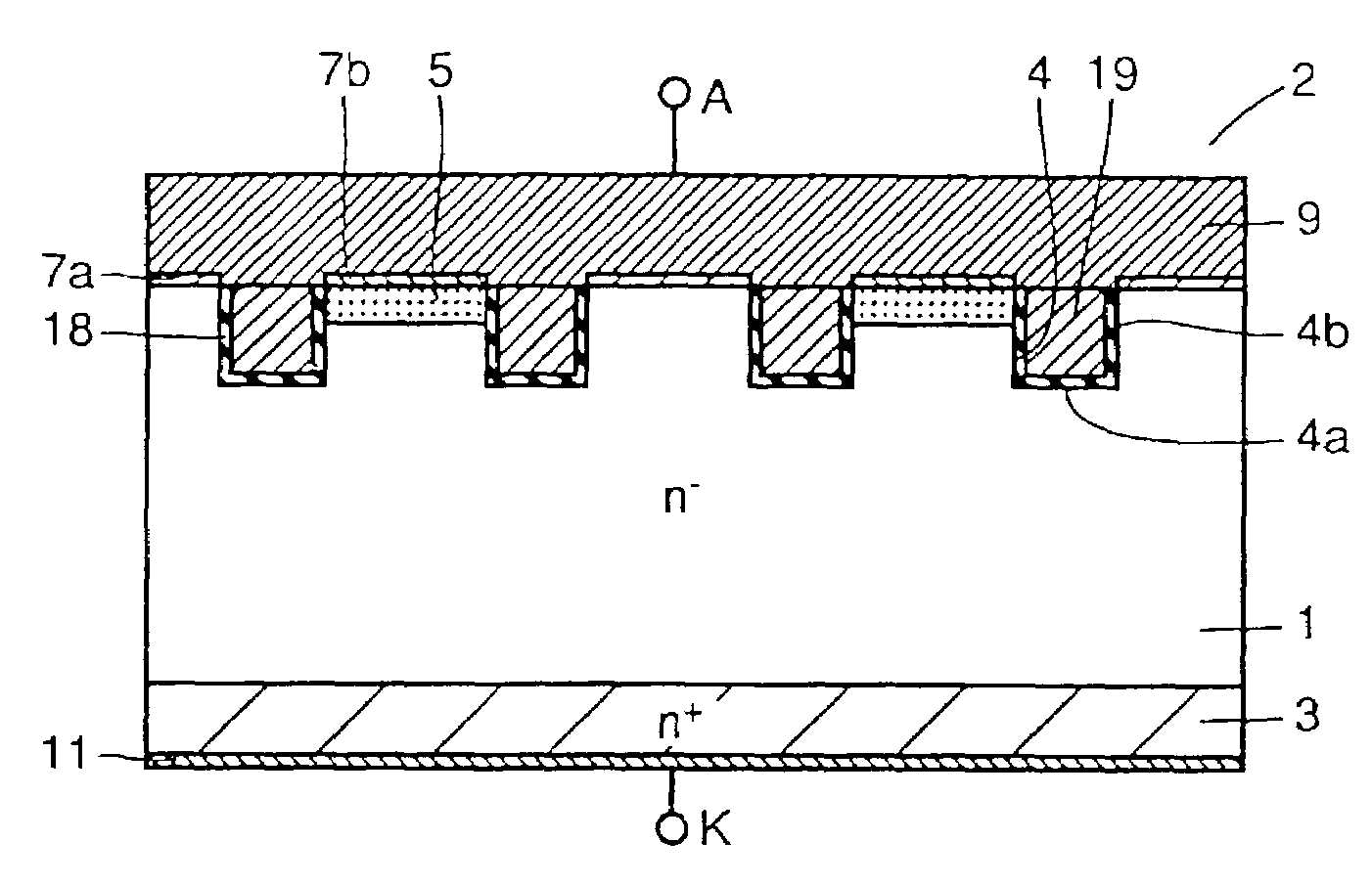
[0082]A diode according to the first embodiment of the invention is described using the accompanying figure. Referring to FIG. 1, a plurality of p anode regions 5 are formed at one surface of an n− substrate 1. Trenches 4 are respectively formed at p anode regions 5. An anode metallic electrode 9 is formed on the one surface of n− substrate 1 to fill trenches 4. A Schottky junction region 7a formed of platinum silicide is formed at an interface between anode metallic electrode 9 and n− substrate 1. On the other surface of n− substrate 1, a cathode metallic electrode 11 is formed with an n+ cathode region 3 therebetween.

[0083]Each p anode region 5 is formed by introduction of a p type impurity into n− substrate 1 and by heat treatment. At the same time that the impurity is thermally diffused from the surface of n− substrate 1 toward its inside, the impurity is also thermally diffused from the surface of n− substrate 1 toward a portion therearound. An initial amount of introducti...

second embodiment

[0088

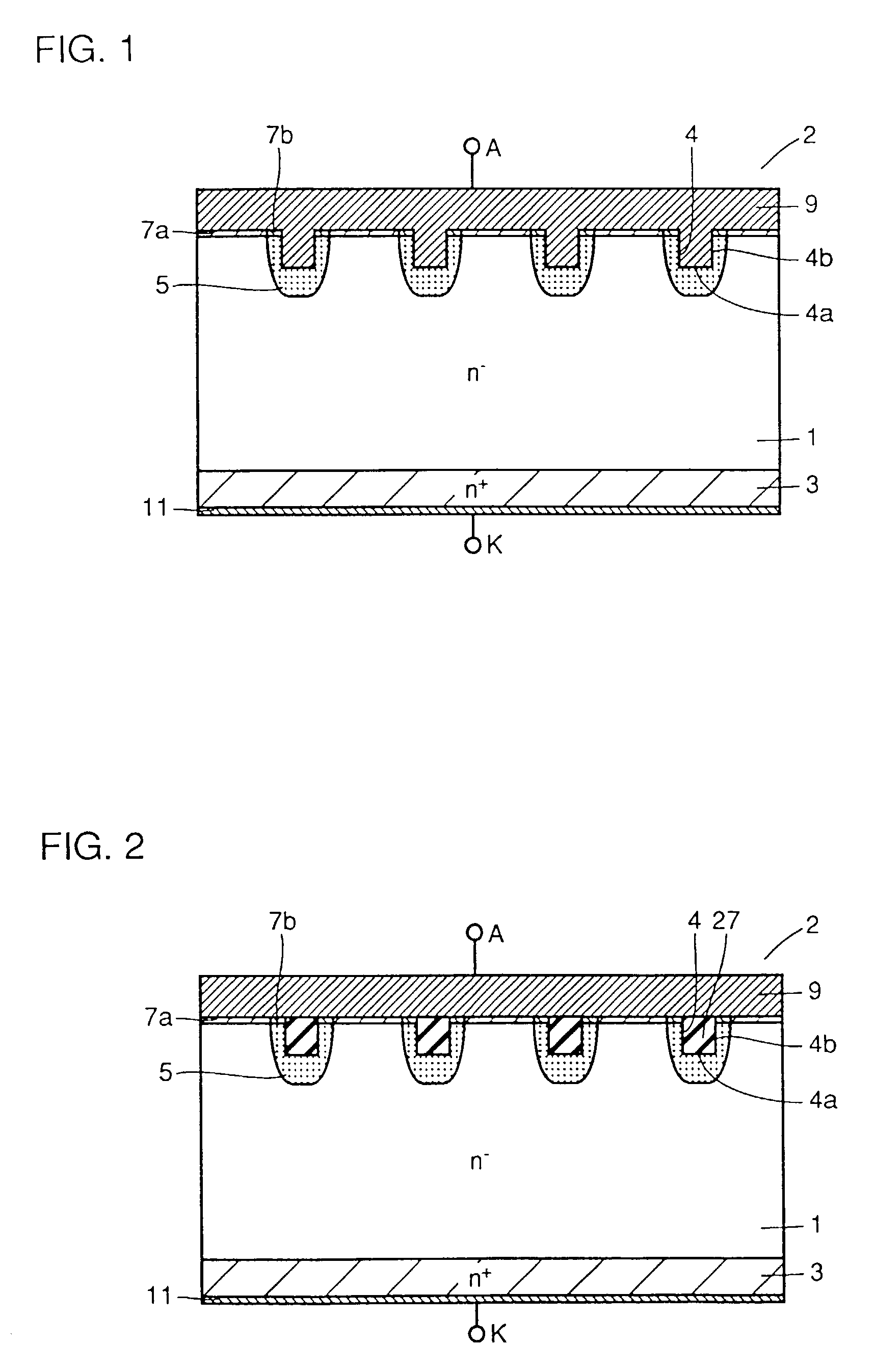
[0089]A diode according to the second embodiment of the invention is described with reference to drawings. Referring to FIG. 2, a silicon oxide film 27 is embedded in trench 4 formed at each p anode region 5. Structural components other than above are similar to those of the diode shown in FIG. 1 described in the first embodiment, identical components are indicated by the same reference characters and detailed description thereof is omitted.

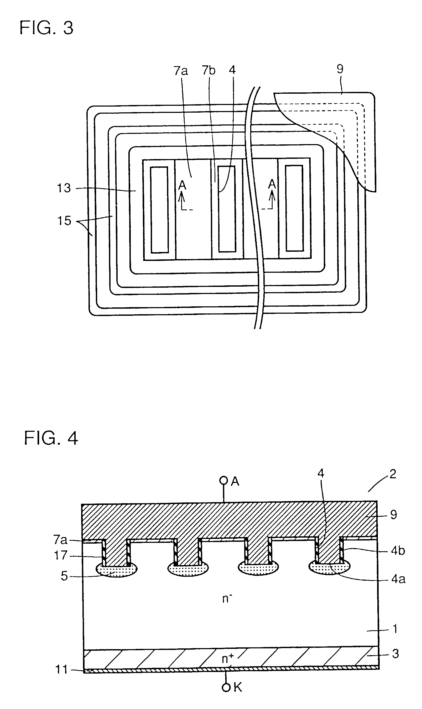
[0090]A two dimensional structure of the diode shown in FIG. 2 is illustrated in FIG. 3 as one example. Referring to FIG. 3, a p anode region is formed around each trench 4, and ohmic junction region 7b between the p anode region and the anode metallic electrode 9 is located. A peripheral p region 13 is formed therearound, and a guard ring 15 for improving insulation property is formed. It is noted that FIG. 2 shows a cross section taken along A—A shown in FIG. 3.

[0091]The operation is next described. In the diode described in the first embo...

third embodiment

[0093

[0094]A diode according to the third embodiment of the invention is described using the accompanying figure. Referring to FIG. 4, a plurality of trenches 4 are formed at one surface of n− substrate 1. A silicon oxide film 17 is formed at a side 4b of each trench 4. P anode region 5 is formed to be in contact with a bottom surface 4a of each trench 4. Anode metallic electrode 9 is formed on n− substrate 1 to fill trench 4. Schottky junction region 7a is provided between anode metallic electrode 9 and n− substrate 1. Anode metallic electrode 9 and p anode region 5 are in ohmic contact with each other at bottom surface 4a of trench. A cathode metallic electrode 11 is formed on the other surface of n− substrate 1 with n+ cathode region 3 therebetween.

[0095]Each p anode region 5 is formed by the thermal diffusion of the p-type impurity introduced into bottom surface 4a of trench as described in the first embodiment. An amount of introduction of the impurity and a condition of the he...


PUM

PropertyMeasurementUnit
withstand voltageaaaaaaaaaa
conductivityaaaaaaaaaa
concentrationaaaaaaaaaa

Abstract

A plurality of p anode regions are formed at one surface of an n− substrate. A trench is formed in each p anode region. An ohmic junction region is formed between an anode metallic electrode and the p anode region. The p anode region has a minimum impurity concentration at a portion near the ohmic junction region which enables ohmic contact. A cathode metallic electrode is formed at the other surface of the n− substrate with an n+ cathode region interposed. Accordingly, a semiconductor device which has an improved withstand voltage and in which the reverse recovery current is reduced can be obtained.

Description

[0001]This application is a divisional application of U.S. patent application Ser. No. 08 / 988,212, filed Dec. 10, 1997 now U.S. Pat. No. 6,501,146.BACKGROUND OF THE INVENTION[0002]1. Field of the Invention[0003]The present invention relates to a semiconductor device and a method of manufacturing a semiconductor device. The invention particularly relates to a semiconductor device which has a higher withstand voltage and in which the reverse recovery current is reduced, and a method of manufacturing such a semiconductor device.[0004]2. Description of the Background Art[0005]A semiconductor device such as an IGBT (Insulated Gate Bipolar Transistor) is applied to various inverter circuits as a switching element. In order to release the energy stored in an inductive load in the switching process and utilize it as the circulating current, a diode is connected in antiparallel with a main semiconductor device. Such a diode is especially referred to as a flywheel diode.[0006]Excess carriers ...

Claims


Application Information

Patent Timeline
Patent Type & Authority Patents(United States)
IPC IPC(8): H01L21/329H01L29/47H01L29/861H01L29/872
CPCH01L29/66136H01L29/66356H01L29/861H01L29/872H01L29/0619
Inventor HARADA, MASANA
Owner MITSUBISHI ELECTRIC CORP
Why Eureka
Try Eureka