Driver circuit for a display device

Inactive Publication Date: 2005-12-06
CALLAHAN CELLULAR L L C
View PDF5 Cites 10 Cited by
  • Summary
  • Abstract
  • Description
  • Claims
  • Application Information

AI Technical Summary

Benefits of technology

[0009]Therefore, it is an object of the invention to provide a driver circuit that can be tested within the shortest possible period of time and with a very extensive fault coverage.
[0011]The basic idea of the device in accordance with the invention is to provide a defect-oriented test and a method that is suitable for that purpose. The use of additional test hardware that is added to the driving device or driver circuit eliminates the need for numerous individual analog measurements whereas the fault error coverage remains equally high or is even enhanced nevertheless.
[0013]In accordance with the invention there is provided a second switching device whereby the voltage that is selected by the multiplex device can be switched to a selectable test reference potential. This selectable or definable test reference potential is preferably ground. The second switching device connects the voltage that is switched through by the multiplex device to a selectable test reference potential. The second switching device enables the M leads that are no longer driven after the opening of the first switching device to be switched through to the second switching device by control of the multiplex device, said second switching device then switching the lead M thus selected to a fixed potential. In the normal case this potential is adjusted on the selected lead and can be simply and readily monitored. If this fixed potential is not present on the selected lead, it is to be assumed that a faulty driver circuit is involved. This enables simple testing of the functionality of the driver circuit. Any leakage currents between different M leads can be simply detected because, when a special lead MI is selected and switched through to the second switching device, any leakage current present can be dissipated via the second lead, so that the necessary level would not be detected during the monitoring of the output N or the selected lead MI and the further lead connected thereto in a faulty manner.
[0021]An advantage of the arrangement in accordance with the invention resides in the fact that the driver circuit for a display device can be tested practically completely digitally, so that the test time is significantly reduced. In comparison with analog measurements, at the same time far simpler test and measuring equipment are required for a digital test. Because of the digital test signal, many test states can be realized so that a very extensive fault coverage can be achieved. Because of the digital nature of the test method, the entire test arrangement is very robust against disturbances by electromagnetic radiation.

Problems solved by technology

Notably portable apparatus such as, for example notebooks, telephones, digital cameras and personal digital assistants (PDA) cannot be realized without using flat displays.
Because such driver circuits have to drive several hundred terminals of the display device, the testing of such a driver circuit is very intricate.
The use of intricate precision measuring apparatus for the test operation also has a negative effect on the price of the finished products.
Because of the digital-to-analog conversion of the digital image signals, the standard test methods for digital logic cannot be used for this driver circuit.
Because it is necessary to generate and test very many different voltage values in a wide range, a test for the driver circuits is very intricate.
The testing of every individual analog voltage value is very time consuming, because each individual value must be programmed and directly tested.
The measurement of a large number of analog outputs with an accuracy of 0.2% of the overall voltage range necessitates the use of very expensive test equipment.
Such a functional test leads to very high test costs and becomes manifest as a very long test time.
The functional tests as described above may also involve faults that arise in the manufacture of the wafers and cannot be detected or not reliably detected.

Method used


Image

  • Driver circuit for a display device
  • Driver circuit for a display device
  • Driver circuit for a display device

Examples


Embodiment Construction

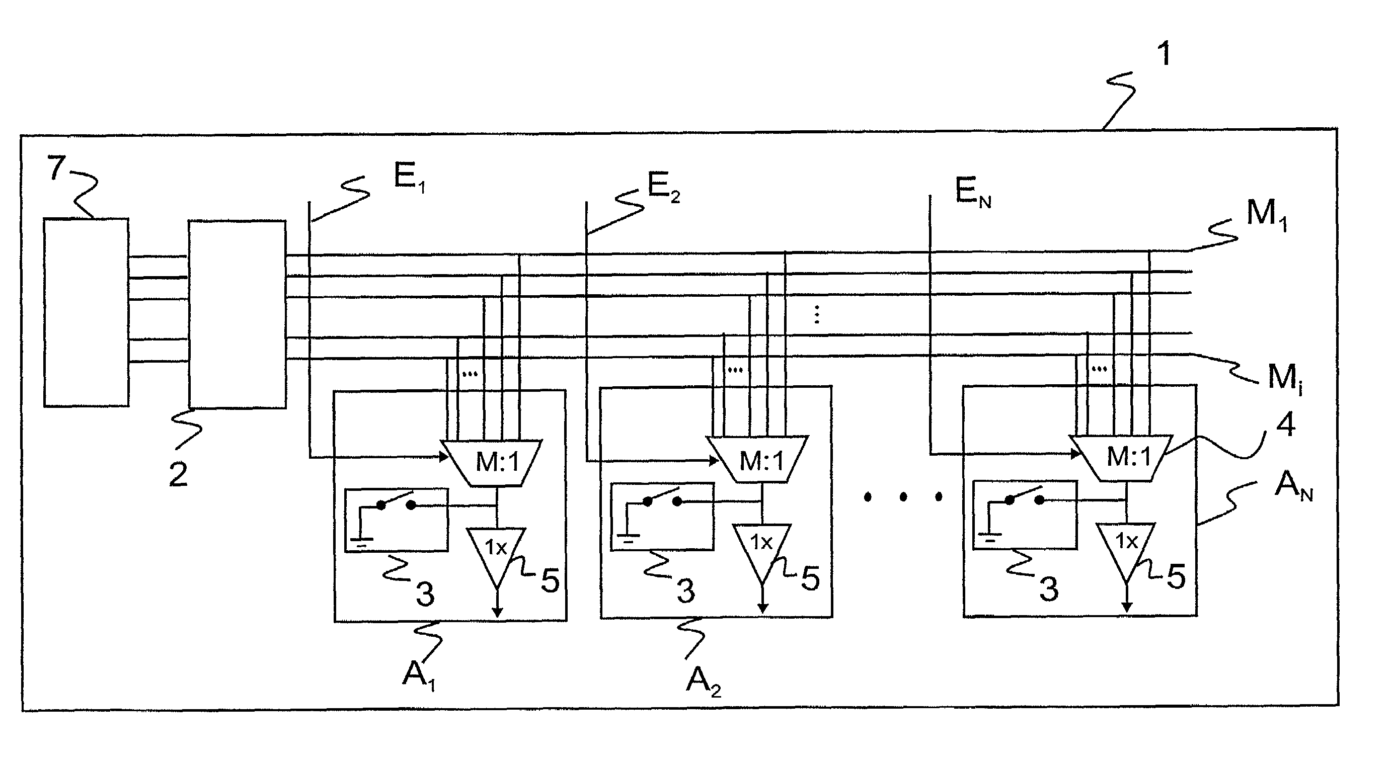
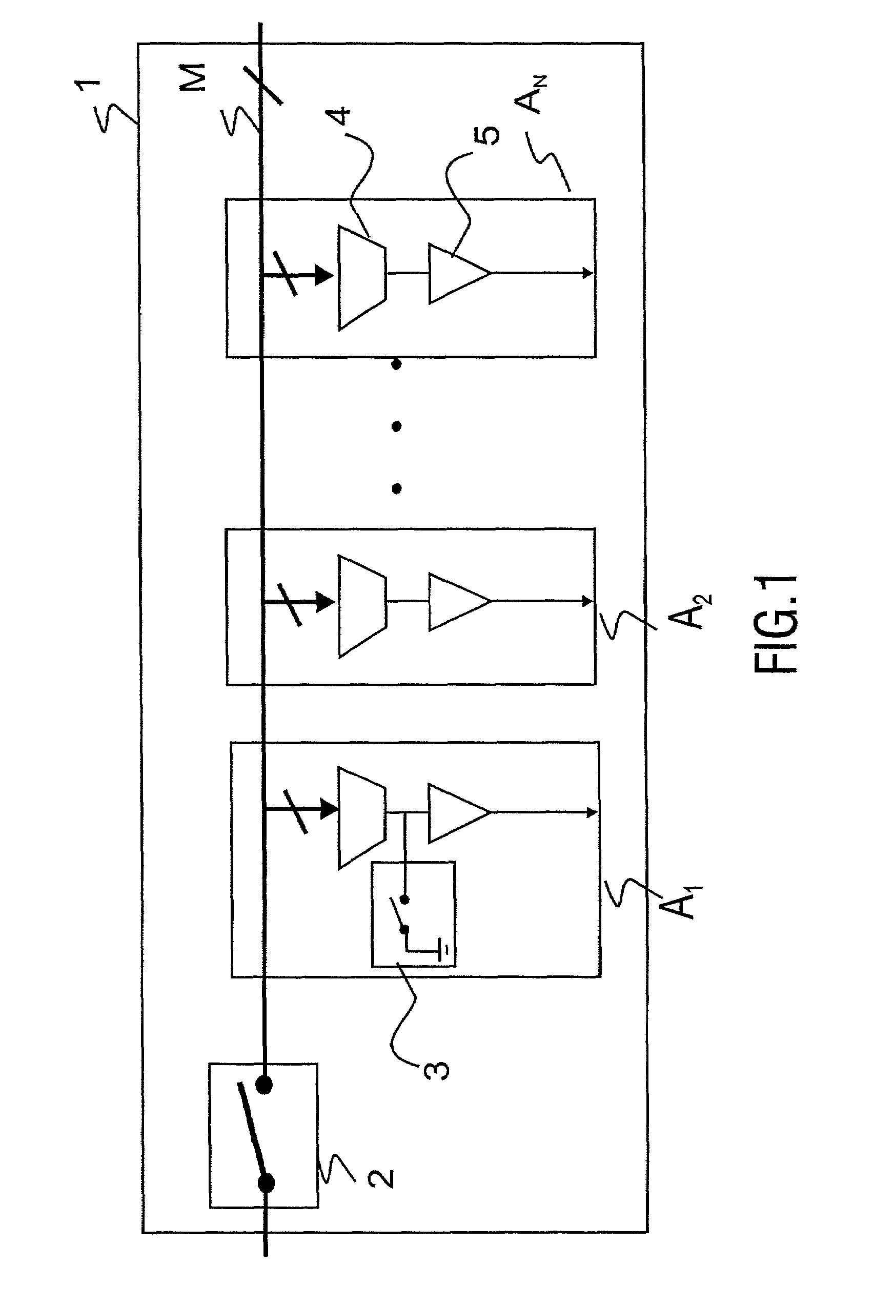
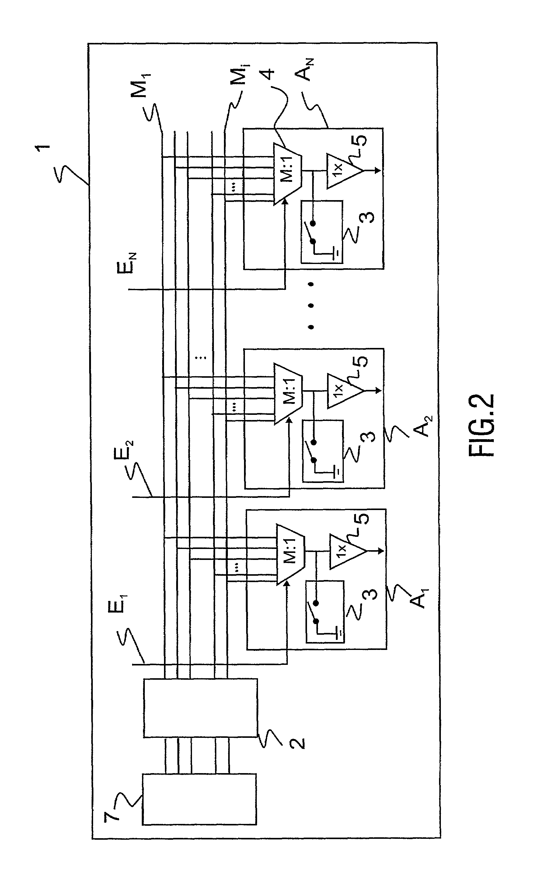
[0028]FIG. 1 shows the M leads that may also be understood to be a voltage bus. The M leads usually include 64 individual leads in the case of a 6-bit D / A converter. The M leads are coupled to the first switching device 2. The first switching device 2 enables interruption of the voltage supply to the M leads. N output stages AN are connected to said M leads, each output stage AN being connected to at least a part of the M leads. Generally speaking, however, all M leads are connected to each output stage AN, because each terminal of a display device must be supplied with each voltage so as to reproduce image information in the corresponding display area. Respective time multiplex devices 4 are provided in the output stages AN. The multiplex devices 4 are arranged to select one of the voltages that are supplied via the M leads. The multiplex devices 4 are coupled to an amplifier 5 that conducts the selected voltage to the output N. A second switching device 3 is provided in at least o...


PUM


Abstract

The invention relates to a device for driving display devices and to a display device that is provided with a driver circuit. The invention also relates to a method of testing driver circuits. Driver circuits of this kind have a decisive effect on the quality of the display devices. Therefore, in order to ensure a good quality, the driver circuit must be extensively tested, that is, with an as short as possible test time and using as few means as possible. In order to make such a test possible, a device for driving the display devices is provided with M leads that are coupled to AN output stages that are provided with at least one multiplex device (4) and at least one amplifier unit (5), the M leads being coupled to a first switching device (2) that enables the interruption of a voltage supply to the M leads, and at least one second switching device (3) being provided in at least one output stage (AN) in order to switch the output stage (AN) to a selectable potential. This enables the use of a test that can be carried out digitally.

Description

BACKGROUND OF THE INVENTION[0001]The invention relates to a device for driving display devices, and to a display device that includes a driver circuit. The invention also relates to a method of testing driver circuits.[0002]In coming years the display technique will play a more and more important part in the field of information and communication. Being the interface between humans and the digital world, the display device is of crucial importance for the acceptance of modem information systems. Notably portable apparatus such as, for example notebooks, telephones, digital cameras and personal digital assistants (PDA) cannot be realized without using flat displays.[0003]Active matrix displays are of particular importance, because such a display device enables fast image changes, for example, in the display of the cursor of a mouse. According to this active matrix LCD technique the image points or pixels are actively driven. The version that is most frequently used utilizes thin film...

Claims


Application Information

Patent Timeline
IPC IPC(8): G09G3/00G09G3/20G09G3/36
CPCG09G3/006G09G3/3688G09G3/2011G09G3/3696G09G2310/027Y10S345/904
Inventor PLANGGER, GUIDO
Owner CALLAHAN CELLULAR L L C
Why Eureka
Try Eureka