Contactless IC card

Inactive Publication Date: 2005-11-08
HITACHI LTD
View PDF9 Cites 17 Cited by
  • Summary
  • Abstract
  • Description
  • Claims
  • Application Information

AI Technical Summary

Benefits of technology

[0010]The present invention is intended to individually optimize a rectifier circuit for data and clock and a rectifier circuit for electric power to facilitate adjustments of data, clock voltage, and supply voltage. For this purpose, a contactless IC card of the present invention comprises a

Problems solved by technology

In such a case, a logical circuit, which receives the supply voltage and data signal from the transmit / receive circuit, is highly susceptible to destruction.
In addition, when the switching element 78 is operated for data transmission, the power diode 73 is largely affected by a change in impedance, which would result in failing to recover a stable supply voltage.

Method used


Image

  • Contactless IC card
  • Contactless IC card
  • Contactless IC card

Examples


Embodiment Construction

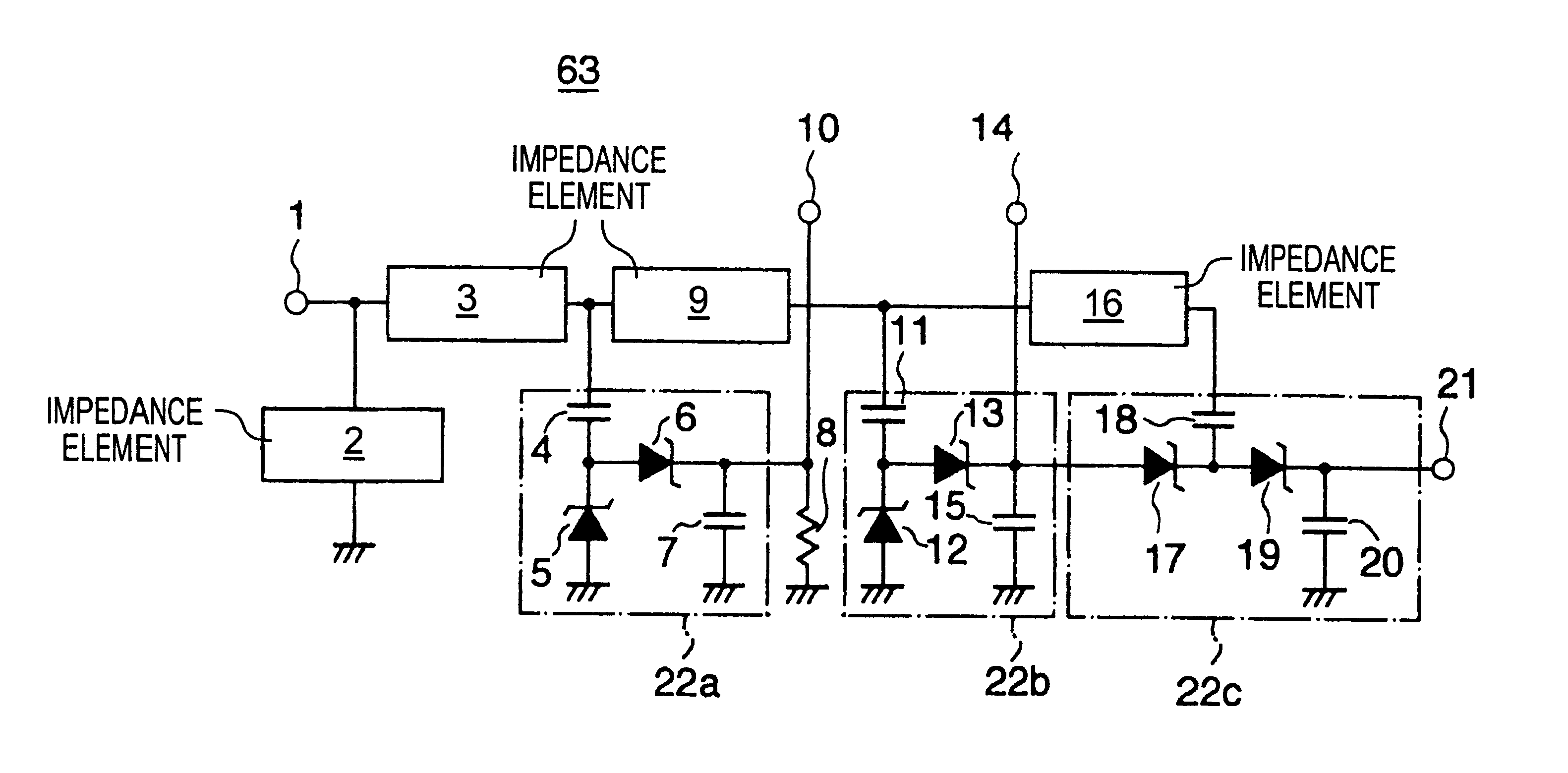
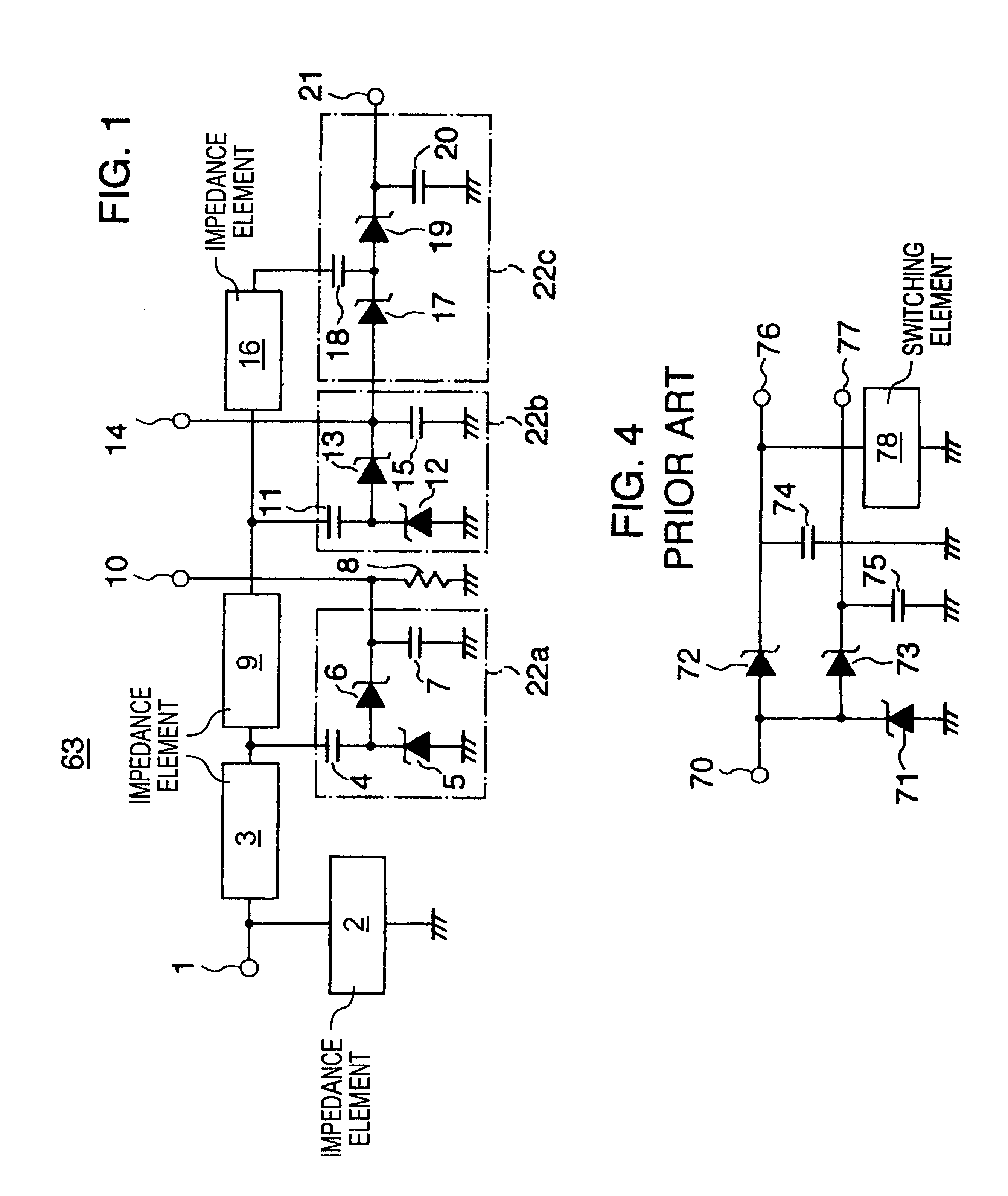
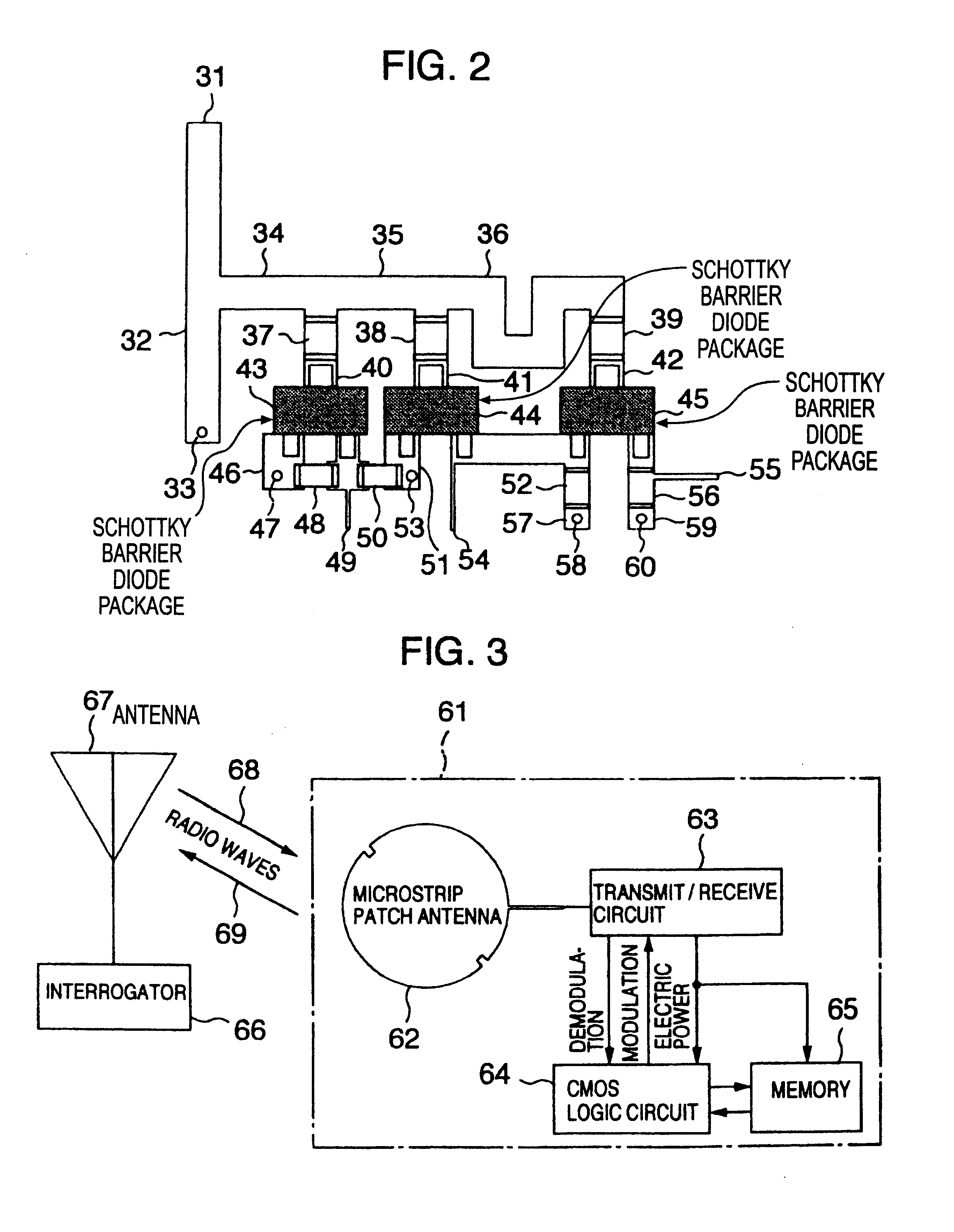
[0016]The configuration of a contactless IC card (tag) according to the present invention is illustrated in FIG. 3.

[0017]An interrogator 66 irradiates an IC card 61 with a downlink signal 68 modulated by a high frequency carrier signal such as microwaves. A microstrip patch antenna 62 has a resonant frequency equal to the carrier frequency. The antenna 62 may be implemented by a dipole antenna, a winding, or a printed coil, depending on the carrier frequency. A carrier signal received by the antenna 62 is inputted to a transmit / receive circuit 63 which demodulates a signal modulated on the carrier signal, and recover supply power from the same. The supply power is supplied to a CMOS logic circuit 64 and a memory 65. The CMOS logic circuit 64 controls the memory 65 to read data from and write data into the memory 65.

[0018]When data stored in the memory 65 is transmitted to the interrogator 66, the impedance of the transmit / receive circuit 63 is changed in accordance with a data signa...


PUM


Abstract

A contactless IC card having an antenna, a transmit / receive circuit for recovering data (clock) and electric power from a carrier signal received by the antenna, a logic circuit operated with the electric power supplied thereto from the transmit / receive circuit, and a memory. The transmit / receive circuit has a rectifier circuit for outputting data (clock) and rectifier circuits for electric power in such a manner that the carrier signal is inputted to each of the rectifier circuit for outputting data (clock) and the rectifier circuit for electric power. With this configuration, high frequency matching can be optimized separately for the rectifier circuit for outputting data (clock) and the rectifier circuit for electric power. It is also possible to separately optimize adjustments to a voltage of recovered data (clock) and a recovered supply voltage.

Description

[0001]This is a continuation application of U.S. Ser. No. 09 / 079,272, filed May 15, 1998 now U.S. Pat. No. 6,570,490.BACKGROUND OF THE INVENTION[0002]The present invention relates to a contactless IC card which does not have a power supply, battery, or sources of signals such as a clock and a carrier. More particularly, the present invention relates to a contactless IC card which is characterized by a transmit / receive circuit adapted to recover a clock for operating signal processing circuits such as logical circuits, memory, and so on, data, and electric power from a high frequency signal derived from an antenna or a coil arranged on the IC card, and to transmit a portion of data stored in the memory in accordance with the received data through the antenna or the coil as transmission data.[0003]In “A Low-Power CMOS Integrated Circuit for Field-Powered Radio Frequency Identification Tags” by D. Friedman et al. published in 1997 IEEE ISSCC (International Solid-State Circuit Conferenc...

Claims


Application Information

Patent Timeline
IPC IPC(8): G06K19/07G06K17/00H04B5/02
CPCG06K19/0713G06K19/0723
Inventor SAITOH, TAKESHISHIDA, MASAAKIISHIFUJI, TOMOAKI
Owner HITACHI LTD
Why Eureka
Try Eureka