Self-aligned method of forming a semiconductor memory array of floating gate memory cells with buried floating gate, pointed floating gate and pointed channel region, and a memory array made thereby

Active Publication Date: 2005-10-25
SILICON STORAGE TECHNOLOGY
View PDF34 Cites 58 Cited by
  • Summary
  • Abstract
  • Description
  • Claims
  • Application Information

AI Technical Summary

Benefits of technology

[0010]The present invention solves the above mentioned problems by providing a self aligned method of forming memory cells with reduced size and novel structure, and a memory cell array formed thereby.

Problems solved by technology

One of the problems facing the manufacturability of semiconductor floating gate memory cell arrays has been the alignment of the various components such as source, drain, control gate, and floating gate.
However, as the dimensions of the floating gate get smaller, the grains of the polysilicon (which are enlarged due to the thermal cycles of the oxidation process) become significant in size compared to the overall size of the floating gate.
The large grain size relative to the size of the floating gate causes the sharp edge to be unevenly formed, which compromises the operation and functionality of the floating gate.
Thus, the asymmetric electric field line density near the floating gate tip 7 limits the maximum voltages usable to erase the memory cells, and limits the scalability of the memory cell size.

Method used


Image

  • Self-aligned method of forming a semiconductor memory array of floating gate memory cells with buried floating gate, pointed floating gate and pointed channel region, and a memory array made thereby
  • Self-aligned method of forming a semiconductor memory array of floating gate memory cells with buried floating gate, pointed floating gate and pointed channel region, and a memory array made thereby
  • Self-aligned method of forming a semiconductor memory array of floating gate memory cells with buried floating gate, pointed floating gate and pointed channel region, and a memory array made thereby

Examples


Embodiment Construction

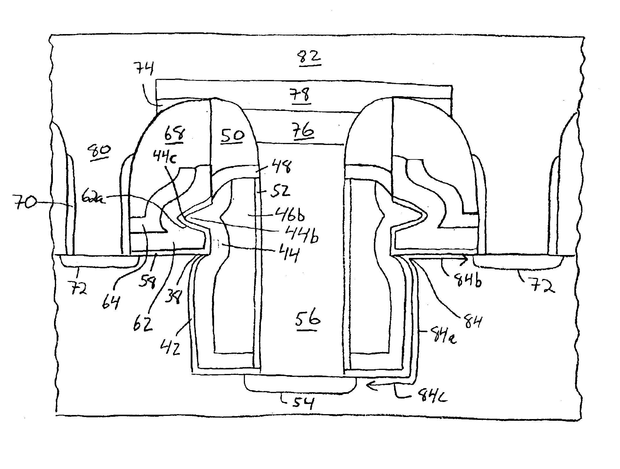
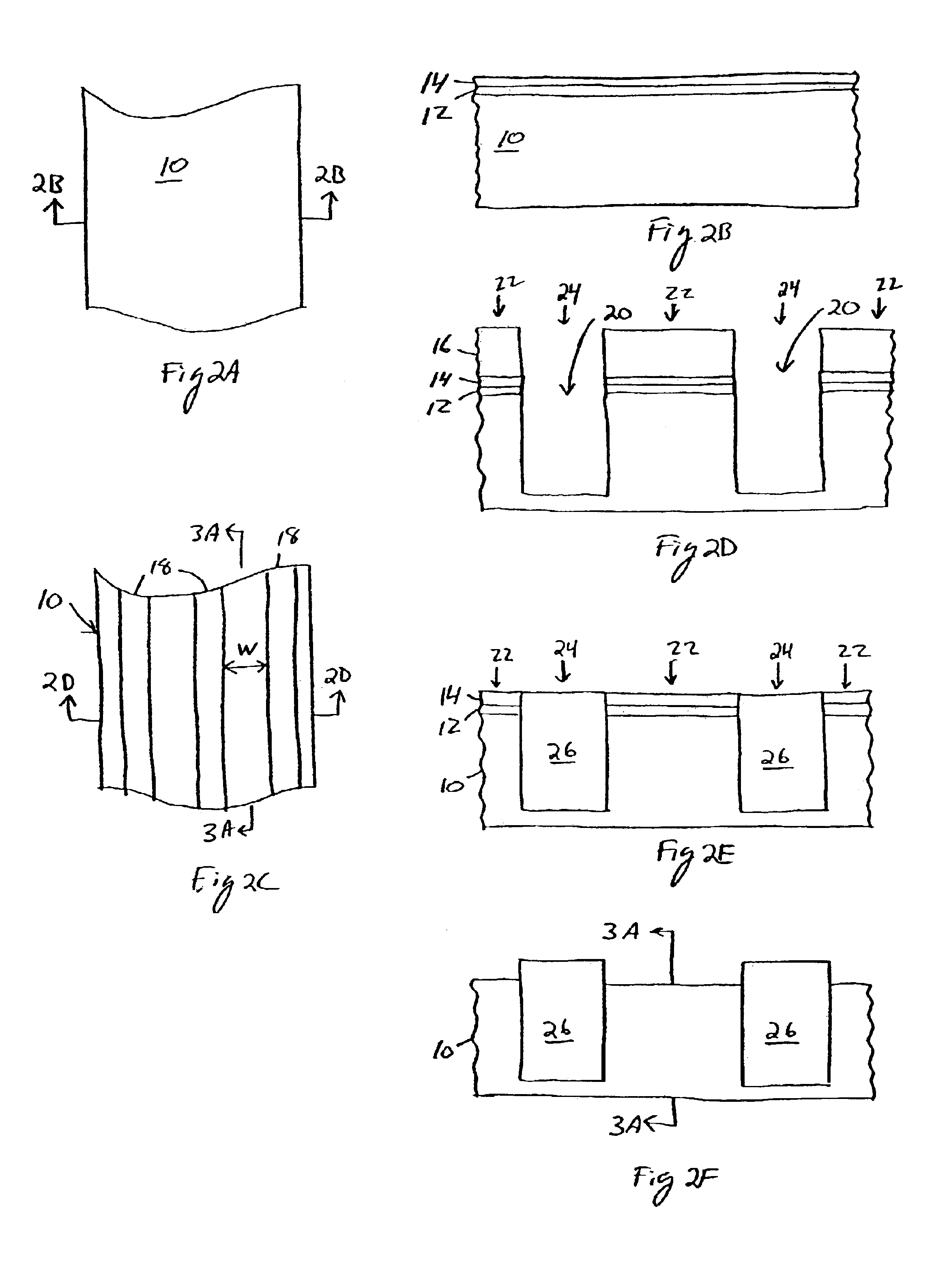
[0027]The method of the present invention is illustrated in FIGS. 2A to 2F and 3A to 3N (which show the processing steps in making the memory cell array of the present invention). The method begins with a semiconductor substrate 10, which is preferably of P type and is well known in the art. The thicknesses of the layers described below will depend upon the design rules and the process technology generation. What is described herein is for the 0.10 micron process. However, it will be understood by those skilled in the art that the present invention is not limited to any specific process technology generation, nor to any specific value in any of the process parameters described hereinafter.

Isolation Region Formation

[0028]FIGS. 2A to 2F illustrate the well known STI method of forming isolation regions on a substrate. Referring to FIG. 2A there is shown a top plan view of a semiconductor substrate 10 (or a semiconductor well), which is preferably of P type and is well known in the art....


PUM


Abstract

A method of forming a floating gate memory cell array, and the array formed thereby, wherein a trench is formed into the surface of a semiconductor substrate. The source and drain regions are formed underneath the trench and along the substrate surface, respectively, with a non-linear channel region therebetween. The floating gate has a lower portion disposed in the trench and an upper portion disposed above the substrate surface and having a lateral protrusion extending parallel to the substrate surface. The lateral protrusion is formed by etching a cavity into an exposed end of a sacrificial layer and filling it with polysilicon. The control gate is formed about the lateral protrusion and is insulated therefrom. The trench sidewall meets the substrate surface at an acute angle to form a sharp edge that points toward the floating gate and in a direction opposite to that of the lateral protrusion.

Description

TECHNICAL FIELD[0001]The present invention relates to a self-aligned method of forming a semiconductor memory array of floating gate memory cells. The present invention also relates to a semiconductor memory array of floating gate memory cells of the foregoing type.BACKGROUND OF THE INVENTION[0002]Non-volatile semiconductor memory cells using a floating gate to store charges thereon and memory arrays of such non-volatile memory cells formed in a semiconductor substrate are well known in the art. Typically, such floating gate memory cells have been of the split gate type, or stacked gate type.[0003]One of the problems facing the manufacturability of semiconductor floating gate memory cell arrays has been the alignment of the various components such as source, drain, control gate, and floating gate. As the design rule of integration of semiconductor processing decreases, reducing the smallest lithographic feature, the need for precise alignment becomes more critical. Alignment of vari...

Claims


Application Information

Patent Timeline
IPC IPC(8): H01L21/28H01L21/336H01L21/70H01L29/66H01L29/40H01L21/02H01L29/423H01L21/8247H01L29/788H01L27/115H01L29/792
CPCH01L21/28273H01L27/11521H01L29/42336H01L29/66825H01L29/7885H01L29/40114H10B41/30
Inventor CHEN, BOMYLEE, DANA
Owner SILICON STORAGE TECHNOLOGY
Why Eureka
Try Eureka