
Solid image-pickup device having a micro lens array and method of manufacturing the same

a micro lens array and solid image technology, applied in the direction of radio frequency controlled devices, instruments, television systems, etc., can solve the problems of a large lens gap, a marked increase in manufacturing costs, and a failure to provide a stable production technology of mass production level

Inactive Publication Date: 2005-09-27
TOPPAN PRINTING CO LTD
View PDF19 Cites 19 Cited by
  • Summary
  • Abstract
  • Description
  • Claims
  • Application Information

AI Technical Summary

Benefits of technology

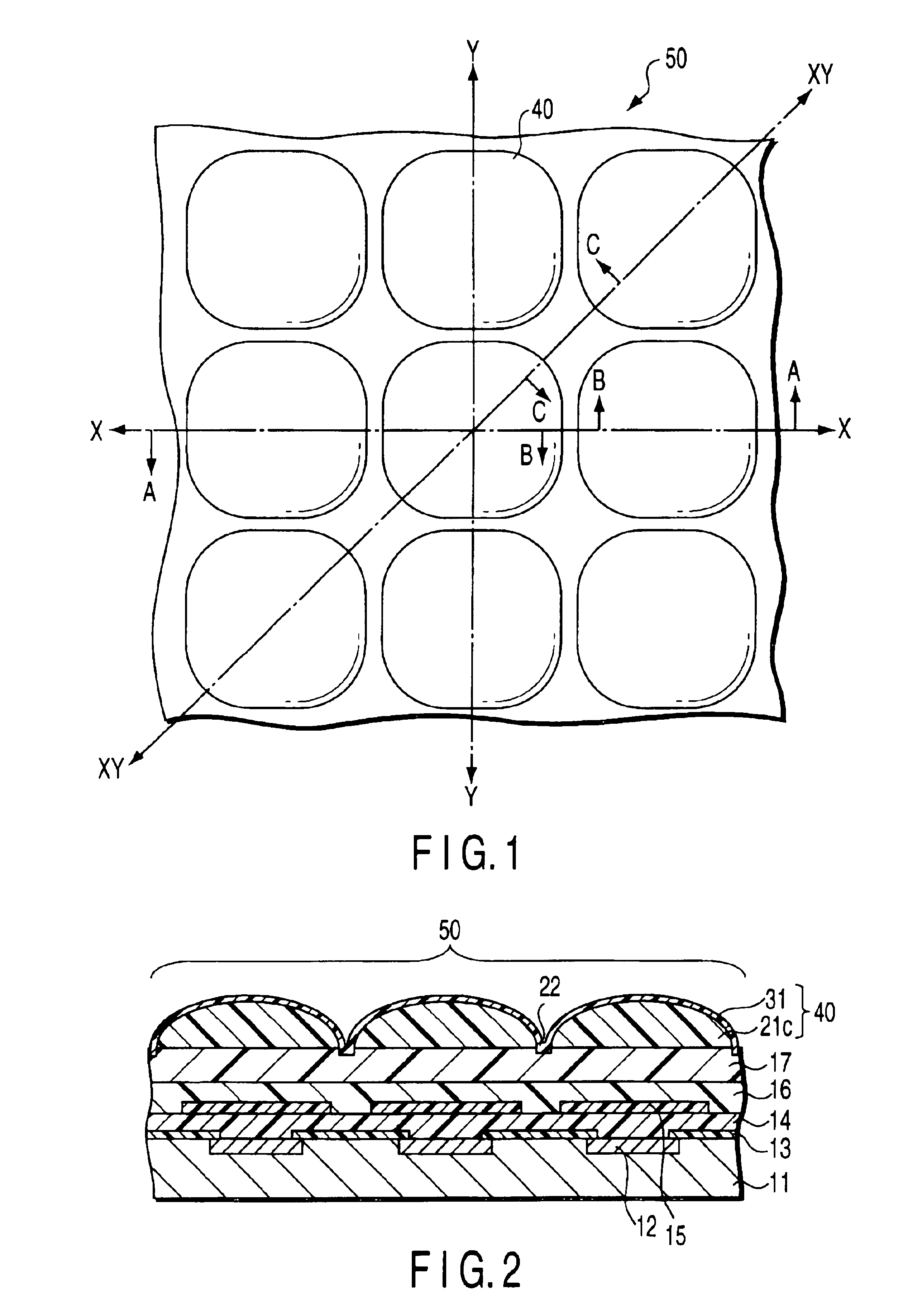
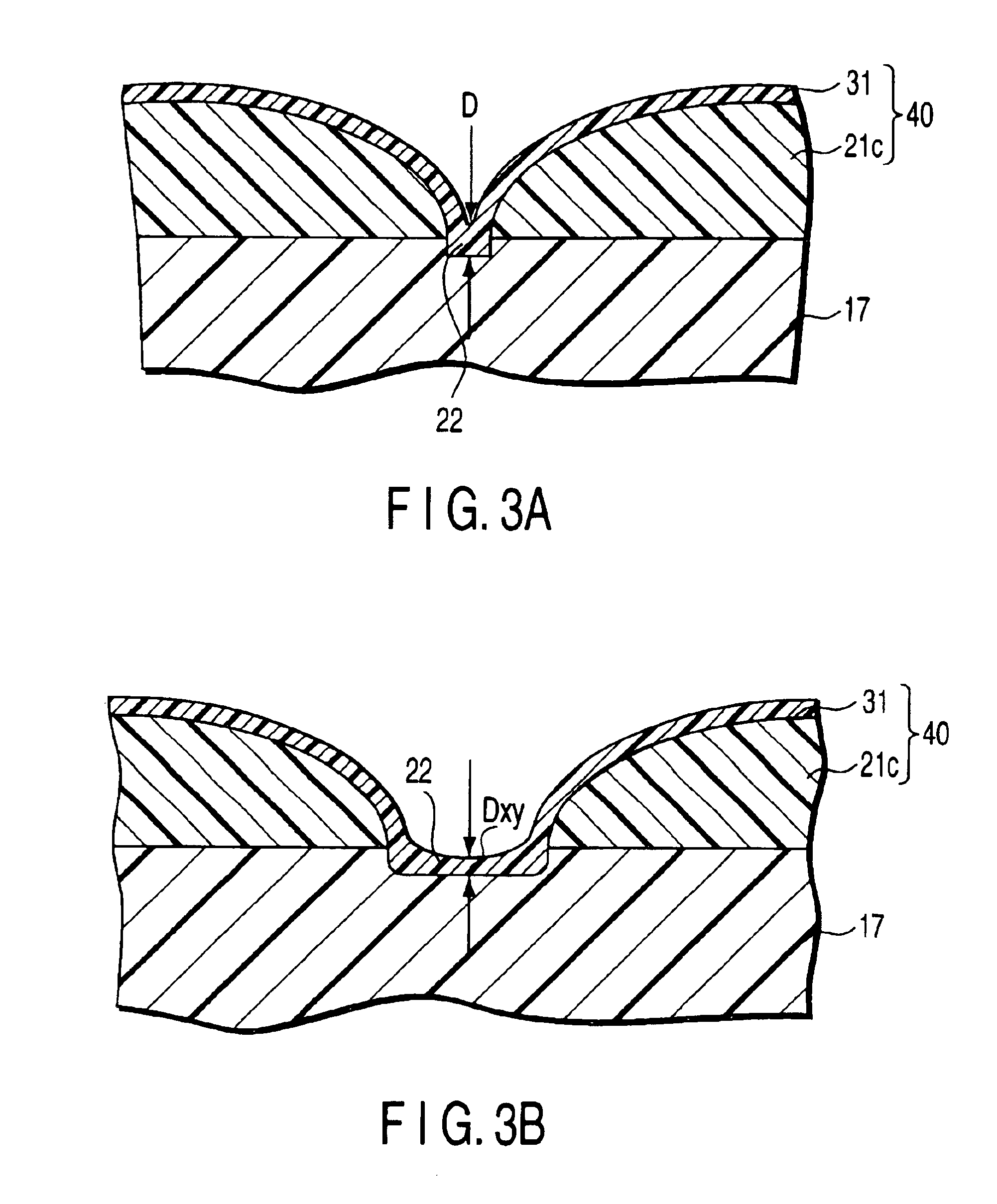
[0016]According to the construction defined in the present invention, it is possible to provide a solid image-pickup device comprising high opening rate micro lenses and the gap not larger than 0.3 μm between the adjacent the micro lenses and a method of manufacturing the same. In addition, it is possible to improve the light collecting effect in the diagonal direction of the micro lens array and to eliminate the lowering of the characteristics of the solid image pickup element caused by the light reflection in the flat portion between the micro lenses in the diagonal direction. As a result, it is possible to provide a solid image pickup element capable of improving the sensitivity and suppressing the smear.

Problems solved by technology

If the lens gap is made 0.3 μm or less in heat flow process, the adjacent micro lenses are connected to each other at the lens edge and the nonuniformity of the photosensitive resin tends to occur, resulting in failure to provide a stable production technology of a mass production level.
The restrictions inherent in the prior art described above lead to the lens gap larger than 0.3 μm.
However, these prior arts necessitate a costly vacuum apparatus and a CVD apparatus and are not simple process, leading to a marked increase in the manufacturing cost.
However, in the trench system, it is difficult to form a small gap between the adjacent micro lenses not larger than 0.3 μm.

Method used


Image

  • Solid image-pickup device having a micro lens array and method of manufacturing the same
  • Solid image-pickup device having a micro lens array and method of manufacturing the same
  • Solid image-pickup device having a micro lens array and method of manufacturing the same

Examples


Embodiment Construction

[0024]Some embodiments of the present invention will now be described with reference to the accompanying drawings. In the following description, the constituents of the present invention having substantially the same function and construction are denoted by the same reference numerals so as to avoid an overlapping description, though an overlapping description is repeated where necessary.

[0025]First of all, the construction of a solid image-pickup device of the present invention will be described with reference to the accompanying drawings.

[0026]FIG. 1 is plan view showing a part of a solid image-pickup device according to one embodiment of the present invention, and FIG. 2 is a cross sectional view along the line A—A shown in FIG. 1. Note that, in the present description, the array direction or the side direction is defined as X- or Y-direction shown in FIG. 1. In addition, the diagonal direction is defined as XY-direction shown in FIG. 1.

[0027]As shown in FIGS. 1 and 2, the solid ...


PUM


Abstract

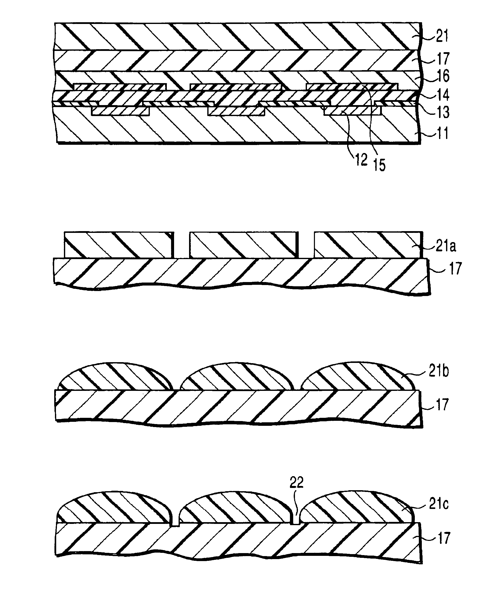
A photovoltaic element, a light shielding portion, a planarized layer, a color filter, another planarized layer and an undercoat layer are formed successively on a semiconductor substrate, followed by forming resin lenses. The undercoat layer positioned between adjacent resin lenses is subjected to an etching treatment with the resin lenses used as a resist mask so as to form ditches extending in the X- and Y-directions and other ditches extending in the XY-direction. Further, a transparent resin layer having a predetermined thickness is formed to cover the resin lenses and the ditches, thereby obtaining a solid image-pickup device comprising a micro lens array including a plurality of micro lenses.

Description

CROSS-REFERENCE TO RELATED APPLICATIONS[0001]This application is based upon and claims the benefit of priority from the prior Japanese Patent Application No. 2000-017329, filed Jan. 26, 2000, the entire contents of which are incorporated herein by reference.BACKGROUND OF THE INVENTION[0002]The present invention relates to a solid image-pickup device represented by a C-MOS, a CCD, etc. and a method of manufacturing the same, particularly, to a solid image-pickup device that permits improving the sensitivity and suppressing the smear by increasing the effective opening rate of a micro lens and a method of manufacturing the same.[0003]The solid image-pickup device comprises the regions contributing to passing the light trough the light receiving element and opto-electric conversion, hereinafter referred to each of the regions as “open portion”. In general, the sensitivity of the light receiving element depends on the size of the open portion. In other words, the small open portion lead...

Claims


Application Information

Patent Timeline
IPC IPC(8): G02B3/00H01L27/14H01L31/062H01L31/06H04N5/225H04N5/335H01L27/146H01L27/148H04N5/359H04N5/369
CPCG02B3/0018G02B3/0056H01L27/14621H01L27/14623H01L27/14627H01L27/14806
Inventor FUKUYOSHI, KENZOISHIMATSU, TADASHIKITAMURA, SATOSHI
Owner TOPPAN PRINTING CO LTD
Learn More