
Clamping and de-clamping semiconductor wafers on an electrostatic chuck using wafer inertial confinement by applying a single-phase square wave AC clamping voltage

a technology of electrostatic chuck and clamping voltage, which is applied in the direction of magnetic bodies, corona discharge, instruments, etc., can solve the problems of reducing process throughput, unable to remove wafers by typical lifting mechanisms, and a considerable amount of surface time, so as to achieve reliable clamping, simple and inexpensive apparatus, and reduce the effect of de-clamping tim

Inactive Publication Date: 2005-09-20
AXCELIS TECHNOLOGIES
View PDF23 Cites 18 Cited by
  • Summary
  • Abstract
  • Description
  • Claims
  • Application Information

AI Technical Summary

Benefits of technology

This method significantly reduces declamping time, ensuring reliable clamping and instantaneous release of the wafer, optimizing for both physical and electrical properties of the electrostatic chuck, and maintaining high throughput without complex electronics.

Problems solved by technology

Declamping or un-sticking the wafer from the chuck surface, however, is a concern in many ESC applications.
For example, after the clamping voltage is turned off, the wafer typically “sticks” to the chuck surface for a considerable amount of time, wherein the wafer cannot be removed by typical wafer lifting mechanisms (e.g., pins extending through the ESC which are operable to lift the wafer from the surface of the dielectric layer).
This wafer declamping problem can reduce the throughput of the process.
It is believed that the wafer-declamping problem occurs when residual charges induced by the clamping voltage remain on the dielectric layer or on a surface of the wafer, therein leading to an undesirable electric field and clamping force.
This reversal voltage, however, is typically 1.5 to 2 times higher than the clamping voltage, and the de-clamping time is still typically quite large.
Such low-frequency sinusoidal AC voltages, however, typically provide low clamping forces, as well as fairly long residual clamping times.
Typically, however, this technique involves quite complicated timing circuits, and do not appear to be optimized for wafer inertial effects, backpressure from a cooling gas, or an overall RC time constant of the electrostatic chuck.

Method used


Image

  • Clamping and de-clamping semiconductor wafers on an electrostatic chuck using wafer inertial confinement by applying a single-phase square wave AC clamping voltage
  • Clamping and de-clamping semiconductor wafers on an electrostatic chuck using wafer inertial confinement by applying a single-phase square wave AC clamping voltage
  • Clamping and de-clamping semiconductor wafers on an electrostatic chuck using wafer inertial confinement by applying a single-phase square wave AC clamping voltage

Examples


Embodiment Construction

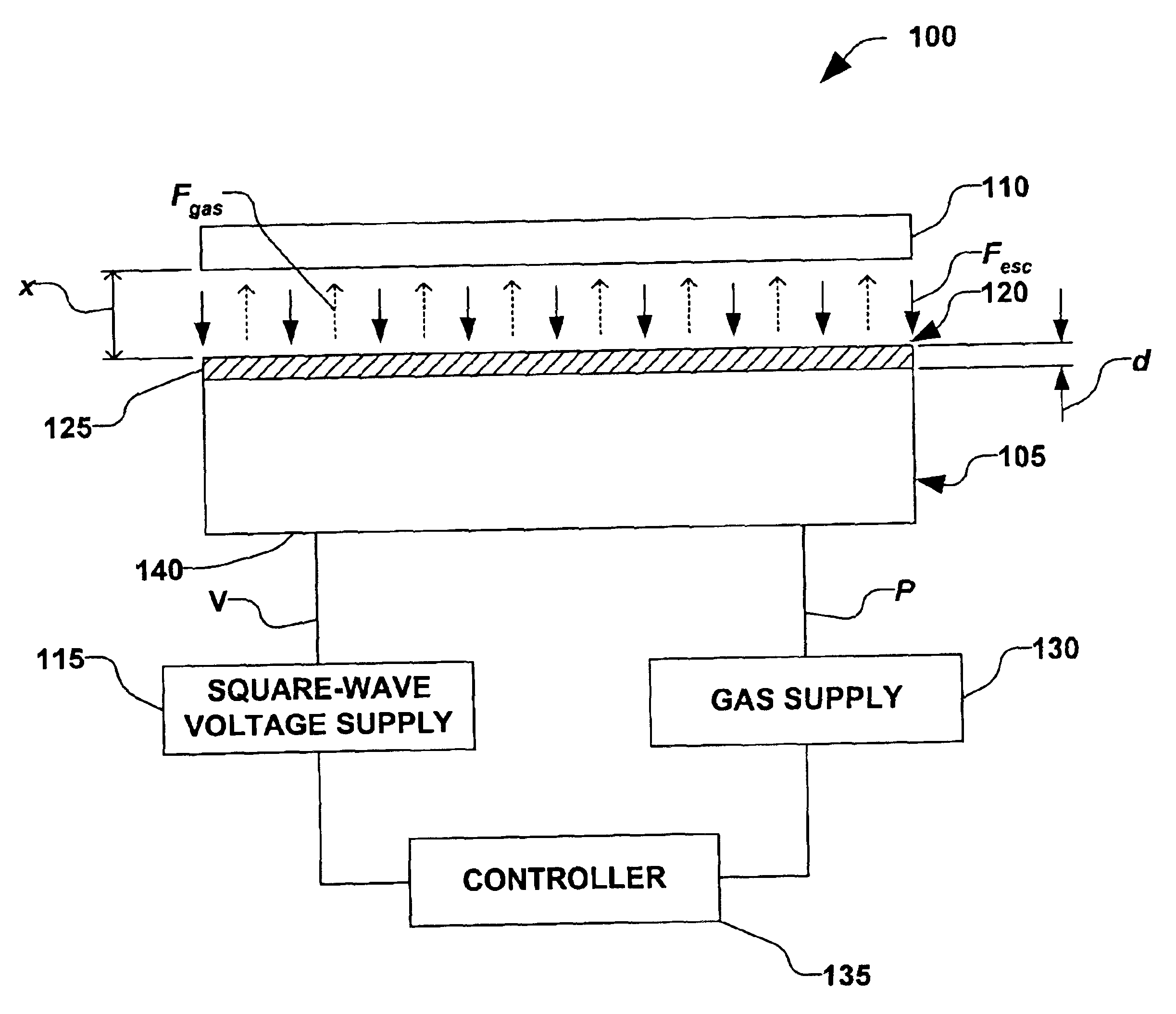
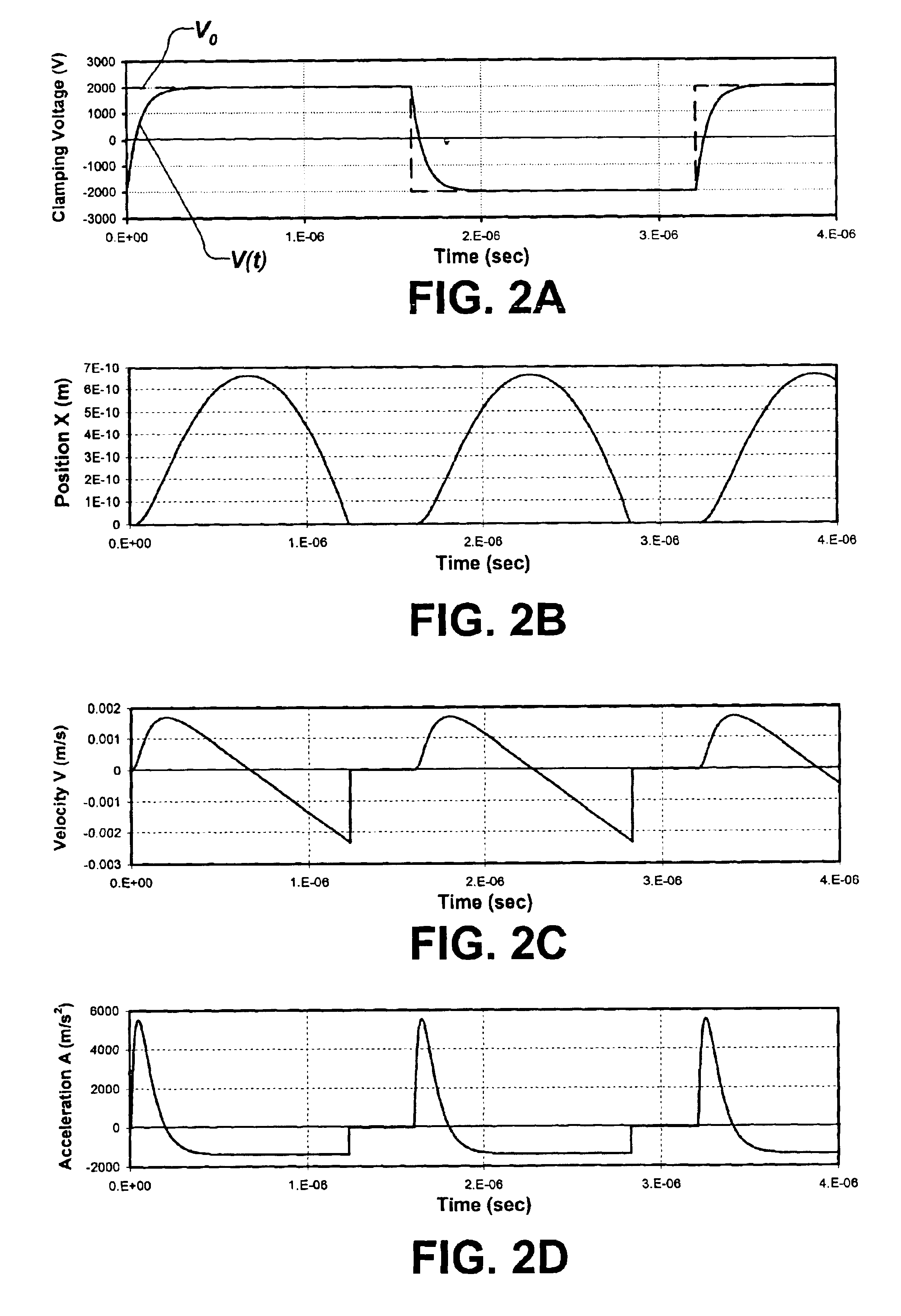
[0019]The present invention is directed towards a system and a method for clamping and de-clamping a wafer utilizing an electrostatic chuck (ESC). Accordingly, the present invention will now be described with reference to the drawings, wherein like reference numerals are used to refer to like elements throughout. It should be understood that the description of these aspects are merely illustrative and that they should not be taken in a limiting sense. In the following description, for purposes of explanation, numerous specific details are set forth in order to provide a thorough understanding of the present invention. It will be evident to one skilled in the art, however, that the present invention may be practiced without these specific details.

[0020]The present invention overcomes challenges of the prior art by providing a system and a method for clamping and de-clamping a wafer (e.g., a semiconductor substrate), wherein a predetermined square-wave voltage is applied to the electr...


PUM

PropertyMeasurementUnit
clamping voltageaaaaaaaaaa
timeaaaaaaaaaa
diameteraaaaaaaaaa

Abstract

The present invention is directed to a method for clamping a wafer to an electrostatic chuck using a single-phase square wave AC clamping voltage. The method comprises determining a single-phase square wave clamping voltage for the electrostatic chuck, wherein the determination is based, at least in part, on an inertial response time of the wafer. The wafer is placed on the electrostatic chuck, wherein a gap between the electrostatic chuck and the wafer is defined. The determined single-phase square wave clamping voltage is then applied, wherein the wafer is generally clamped to the electrostatic chuck within a predetermined distance, while an amount of electrostatic charge is generally not allowed to accumulate, thereby enabling a fast de-clamping of the wafer.

Description

RELATED APPLICATIONS[0001]This application is related to U.S. application Ser. No. 10 / 642,939, filed on Aug. 18, 2003, entitled, “MEMS Based Multi-Polar Electrostatic Chuck” which is incorporated herein by reference, and U.S. application Ser. No. 10 / 661,180, filed on Sep. 12, 2003, entitled, “Clamping and De-clamping Semiconductor Wafers on a J-R Electrostatic Chuck Having a Micromachined Surface by Using Force Delay in Applying a Single-Phase Square Wave AC Clamping Voltage”.FIELD OF THE INVENTION[0002]The present invention relates generally to semiconductor processing systems, and more specifically to a method for clamping a wafer to an electrostatic chuck by applying a single-phase square-wave AC clamping voltage.BACKGROUND OF THE INVENTION[0003]Electrostatic chucks (ESCs) have been utilized in plasma-based or vacuum-based semiconductor processes such as etching, CVD, and ion implantation, etc. for a long time. Capabilities of the ESCs, including non-edge exclusion and wafer temp...

Claims


Application Information

Patent Timeline
Patent Type & Authority Patents(United States)
IPC IPC(8): H01L21/67H01L21/683H02N13/00
CPCH02N13/00H01L21/6833H01L21/687
Inventor KELLERMAN, PETER L.QIN, SHUDIVERGILIO, WILLIAM F.
Owner AXCELIS TECHNOLOGIES
Learn More