Multiplexer

a multi-channel, multi-channel technology, applied in the field of multi-channel devices, can solve the problems of large insertion loss, large insertion loss poses a serious problem, and the element dimension is increased to interfere with the miniaturization, so as to reduce the insertion loss and improve the isolation characteristics

Inactive Publication Date: 2005-08-09
UBE IND LTD
View PDF11 Cites 17 Cited by
  • Summary
  • Abstract
  • Description
  • Claims
  • Application Information

AI Technical Summary

Benefits of technology

[0007]In view of the foregoing, an object of the present invention is to provide a compact and high-performance multiplexer which enables further miniaturization, a reduction of insertion losses and a further improvement of isolation characteristics.
[0013]The multiplexer of the present invention has the combined three demultiplexing filter circuits, and the input of the RF signals f1 to f4 (where f1<f2<f3<f4) belonging to the four frequency bands different from one another is separated into the RF signals f1 and f2 of the lower frequency bands and the RF signals of f3 and f4 of the higher frequency bands by the first demultiplexing filter circuit, the RF signals f1 and f2 of the lower frequency bands output from the first demultiplexing filter circuit are separated into the RF signal f1 and the RF signal f2 by the second demultiplexing filter circuit, and the RF signals f3 and f4 of the higher frequency bands output from the first demultiplexing filter circuit are separated into the RF signal f3 and the RF signal f4 by the third demultiplexing filter circuit. By this structure, the number of stages of cascade-connected demultiplexing filter circuits can be reduced to two, thereby achieving a reduction of insertion losses. Further, the first demultiplexing filter circuit may comprise the low-pass filter and the high-pass filter, the second demultiplexing filter circuit may comprise the low-pass filter for passing the RF signal f1 and the filter of the combination of low-pass and band elimination filters for taking out the RF signal f2, and the third demultiplexing filter circuit may comprise the high-pass filter for passing the RF signal f4 and the filter of the combination of high-pass and band elimination filters for taking out the RF signal f3. Thus, isolation characteristics of each RF signal can be improved, the number of notch circuits can be reduced, and an attenuation load of each demultiplexing filter circuit can be reduced. By forming these demultiplexing filter circuits into one laminated structural body, a compact and high-performance multiplexer which has small insertion losses and improved isolation characteristics is provided.
[0014]Further, also by using a band-pass filter in place of the combination filter including the band elimination filter in each of the second demultiplexing filter circuit and the third demultiplexing filter circuit, a high-performance multiplexer having similar effects is provided.

Problems solved by technology

However, in the aforementioned demultiplexing filter circuit where the three demultiplexing filter circuits are cascade-connected, while the four frequency bands can be separated as described above, there are some problems described below.
First, the RF signals f3 and f4 are passed through the three demultiplexing filter circuits, creating a problem of a large insertion loss in signal.
Thus, a large insertion loss poses a serious problem.
In the case of simply using three normal individual demultiplexing filter elements and connecting the elements, element dimensions are increased to interfere with miniaturization.
Furthermore, if a plurality of frequency bands are close to one another, there is a problem of insufficient separation of RF signals.

Method used


Image

  • Multiplexer
  • Multiplexer
  • Multiplexer

Examples


first embodiment

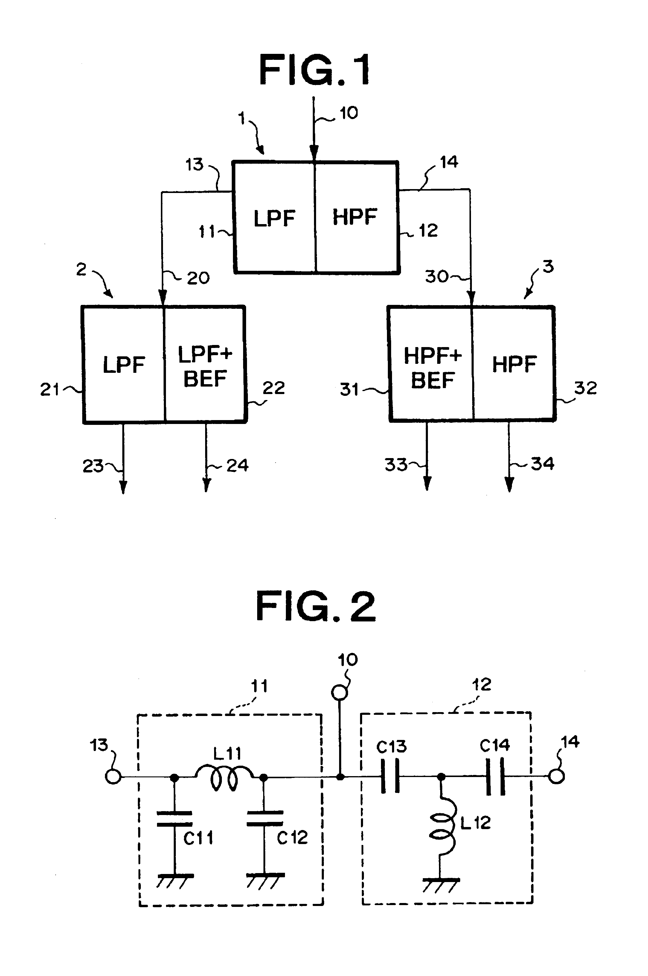
[0045]The aforementioned multiplexer of the first embodiment is preferably formed in a laminated or stacked structural body. That is, preferably, the inductance components L11, L12, L21 to L24, L31 to 34 and the capacitance components C11 to C14, C21 to 28, C31 to 38 of the first demultiplexing filter circuit 1, the second demultiplexing filter circuit 2 and the third demultiplexing filter circuit 3 are formed by using patterned conductive layers constituting the laminated structural body.

[0046]A perspective view of such a laminated structural body is shown in FIG. 9, and an exploded perspective view thereof is shown in FIG. 8. The laminated structural body has external ground (GND) terminals 101, 103, 104, 106, 108, 110, 112, an external input terminal 102, and external output terminals 105, 107, 109, 111, which are formed of the patterned conductive layers.

[0047]This laminated structural body can be prepared by using a sheet laminating method described below.

[0048]First, a ceramic...

second embodiment

[0072]As described above, also it is possible to obtain the high-performance multiplexer where sufficient miniaturization is possible, insertion losses are small, isolation characteristics are improved more, and the four RF signals are separated into the respective components.

[0073]In the second embodiment, the band pass filters are used in place of both of the combination filters including the band elimination filters used in the second demultiplexing filter circuit 2 and the third demultiplexing filter circuit 3 of the circuitry of the first embodiment. However, according to the present invention, the band pass filter may be used in place of only one of the combined filters including the band elimination filters used in the second demultiplexing filter circuit 2 and the third demultiplexing filter circuit 3 of the circuitry of the first embodiment. Also by this way, it is possible to obtain effects similar to those of the first embodiment and the second embodiment.


PUM


Abstract

Four frequency components (f1 to f4) (where, f1<f2<f3<f4) are input into a port (10) of a first demultiplexing filter circuit (1), and demultiplexed into low frequency components (f1 and f2) and high frequency components (f3 and f4), and input in a port (20) of a second demultiplexing filter circuit (2) and a port (30) of a third demultiplexing filter circuit (3), respectively. The frequency components (f1 and f2) are demultiplexed into the component (f1) and the component (f2) by the second demultiplexing filter circuit (2), and output from a port (23) and a port (24), respectively. The frequency components (f3 and f4) are demultiplexed into the component (f3) and the component (f4) by the third demultiplexing filter circuit (3), and output from a port (33) and a port (34), respectively. The first demultiplexing filter circuit (1) comprises a low-pass filter (11) and a high-pass filter (12), the second demultiplexing filter circuit (2) comprises a low-pass filter (21) and a combined filter (22) of a combination of a low-pass filter and a band elimination filter, and the third demultiplexing filter circuit (3) comprises a combined filter (31) of a combination of a high-pass filter and a band elimination filter and a high-pass filter (32). These demultiplexing filter circuits are formed of a stacked structure.

Description

[0001]This application is a 371 of PCT / JP01 / 11272 filed on Dec. 21, 2001, published on Jul. 4, 2002 under publication number WO 02 / 052724 A1 and claims priority benefits of Japanese Patent Application No. 2000-390468 filed Dec. 22, 2000.TECHNICAL FIELD[0002]The present invention relates to a multiplexer used for a mobile communication device such as a portable terminal of a cellular phone system.BACKGROUND ART[0003]Popularization of the cellular phone system has been spectacular in recent years, and improvements have been pursued in functions of the portable terminal used in the cellular phone system. As one of such improvements, a cellular phone system has been presented, which uses a dual band portable terminal to enable communications in two frequency bands at one portable terminal. Further, a cellular phone system has been presented, which uses a multifunctional portable terminal based on positioning by a global positioning system (GPS), an addition of a blue tooth (BT) etc. To ...

Claims


Application Information

Patent Timeline
IPC IPC(8): H03H7/01H03H7/46H03H7/075H03H7/00
CPCH03H7/0115H03H7/075H03H7/1791H03H7/463H01P1/213H03H2001/0085
Inventor FURUYA, SHINJIFURUYA, YOSHIKOICHIKAWA, HIROSHIOYAMA, RYUJIIWASHITA, KAZUKIFUKUDA, KOICHI
Owner UBE IND LTD
Why Eureka
Try Eureka