Coplanar line, and a module using the coplanar line

a technology of coplanar line and coplanar line, which is applied in the direction of instruments, waveguides, and semiconductor/solid-state device details, etc., can solve the problems of degrading the transmitting characteristic of the signal line, and achieve the effect of preventing the degradation of the quality of the signal

Inactive Publication Date: 2005-08-09
SUMITOMO ELECTRIC IND LTD
View PDF5 Cites 4 Cited by
  • Summary
  • Abstract
  • Description
  • Claims
  • Application Information

AI Technical Summary

Benefits of technology

[0007]By setting a relation between the width of the signal line and the distance to the ground plane to be an exponential relation, impedance of the signal line can be maintained to be characteristic impedance, whereby quality of a signal transmitted on the the coplanar line can be prohibited from degradation.
[0008]Another aspect of the present invention relates to an optical module comprises an optical semiconductor device, an electrical semiconductor device and a coplanar line. The coplanar line is electrically connected the electronic semiconductor device and has a feature that a distance between the signal line and a pair of ground planes, which sandwiches the signal line therebetween, varies exponentially with a width of the signal line. The electrical signal output from the electronic semiconductor device or entered thereinto is transmitted on the coplanar line, whereby quality of the signal can be prohibited from degradation.
[0012]Another aspect of the present invention relates to an electronic module comprising an electronic semiconductor device and a coplanar line. The coplanar line is electrically connected the electronic semiconductor device and has a feature that a distance between the signal line and a pair of ground planes, which sandwiches the signal line therebetween, varies exponentially with a width of the signal line. The electrical signal output from the electronic semiconductor device or entered thereinto is transmitted on the coplanar line, whereby quality of the signal can be prohibited from degradation.
[0014]The module may further include a base made of a metal, the substrate, on which the coplanar line and the electronic device is provided, is provided on the base, whereby quality of the signal can be prohibited from degradation. The substrate may has an opening, thorough which the electrical semiconductor device is directly mounted onto the base.

Problems solved by technology

However, such configuration may degrade a transmitting characteristic of the signal line due to impedance mismatching of the signal line.

Method used


Image

  • Coplanar line, and a module using the coplanar line
  • Coplanar line, and a module using the coplanar line
  • Coplanar line, and a module using the coplanar line

Examples


Embodiment Construction

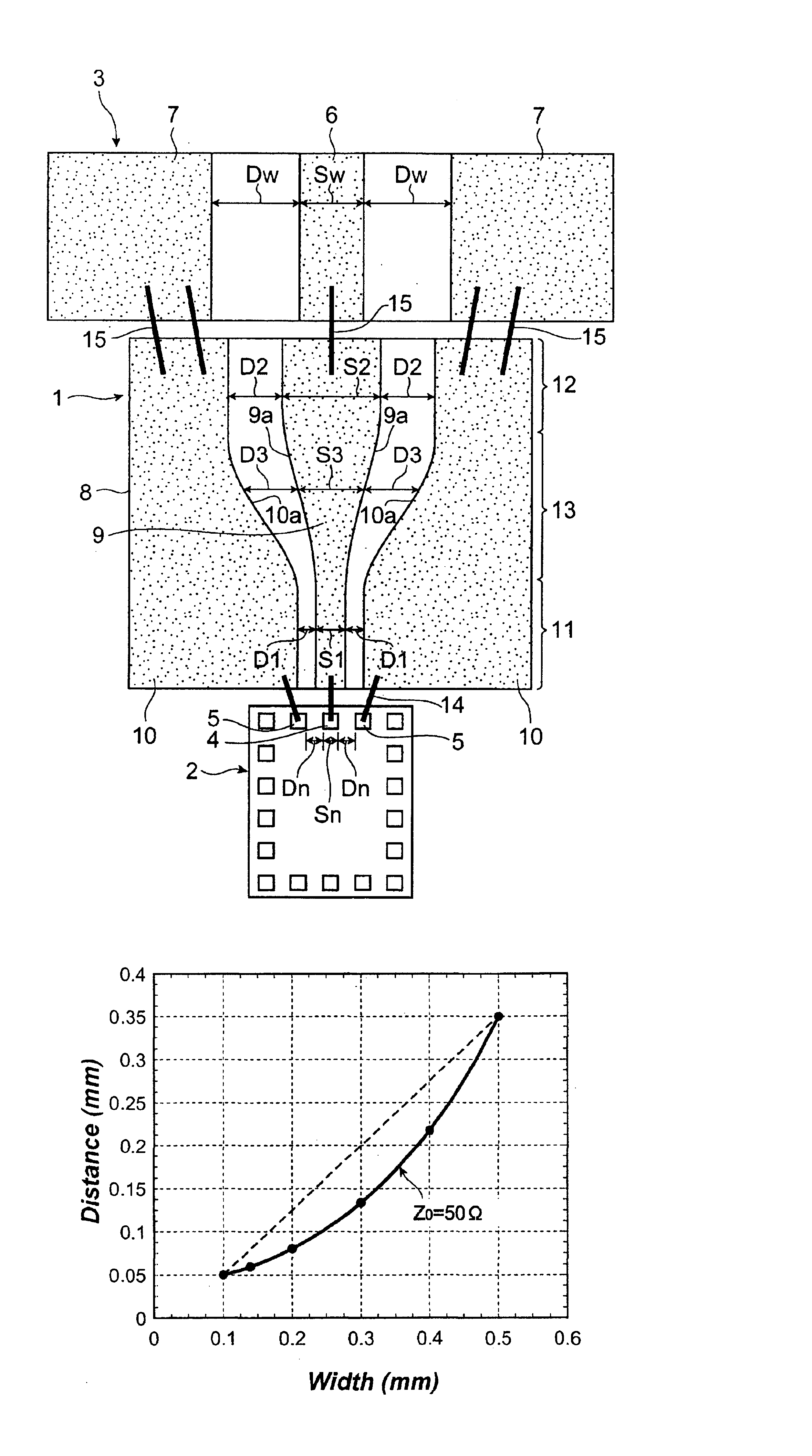
[0023]Preferred embodiments of a configuration of coplanar line, that of a transmission module and a package thereof will be described as referring to accompanied drawings.

[0024]FIG. 1 shows a plan view showing a configuration of a coplanar line of the present embodiment. In FIG. 1, a substrate 1 of the coplanar line connects a semiconductor device 2 to another substrate 3 placed in the outside of the package.

[0025]The semiconductor device 2 has a signal terminal 4 for transmitting a signal, and a pair of ground terminals 5 arranged in both sides of the signal terminal. The substrate 3 has a signal line 6 and a pair of ground planes 7 arranged in both sides of the signal line 6. An distance Dw between the signal line 6 and one of the ground plane 7 at the substrate 3 is greater than an distance between the signal terminal 4 and one of the ground terminal 5 at the semiconductor device. Furthermore, the width Sw of the signal line 6 at the substrate 3 is also greater than that Sn of t...


PUM


Abstract

This invention provides a newly designed coplanar line and an optical module or an electrical module using the coplanar line. The coplanar line comprises a signal transmission line and a pair of ground planes, each are arranged both sides of the signal transmission line. The coplanar line comprises three portions. The first portion has a relatively narrow width of the signal transmission line and the distance to the ground planes. The second portion has a relatively wider width of the signal transmission line and the distance to the ground planes, and the third portion smoothly connects the first portion to the second portion. The distance to the ground planes in the third portion has an exponential relation to the width of the signal transmission line thereof.

Description

BACKGROUND OF THE INVENTION[0001]1. Field of the Invention[0002]This invention relates to a coplanar line and an assembly installing the coplanar line.[0003]2. Related Prior Art[0004]An electrical and an optical package, in which a semiconductor device is assembled, have a coplanar line to connect the device with an outside of the package. The coplanar line comprises a signal line and ground planes disposed in both sides of the signal line. Since intervals between terminals of the semiconductor device is so narrow, for example smaller than a few hundred microns meters, the interval between the signal line and the ground plane must be formed in narrow to match the interval between the terminals of the semiconductor device. On the other hand in the outside of the package, the interval and the width thereof become a few millimeters to take the connection to the motherboard into account. Accordingly, it is necessary for the coplanar line to provide a portion where the width of the signa...

Claims


Application Information

Patent Timeline
Patent Type & Authority Patents(United States)
IPC IPC(8): G02B6/42H01L23/02H01L23/58H01L23/057H01L23/66H01L23/12H01P3/02H01P5/02H01P5/08
CPCG02B6/4201H01L23/057H01L23/66H01L2223/6611H01L2223/6627H01L2224/48227H01L2224/4911H01L2224/49171H01L2924/01079H01L2924/15173H01L2924/1903H01L2924/19107H01L2924/3011H01L24/48H01L24/49H01L2924/00H01L2924/12042H01L2924/12043H01L24/45H01L2224/05599H01L2224/45144H01L2224/85399H01L2924/00014G02B6/4279H01L2224/45015H01L2924/207
Inventor ARAYA, YOSHIHISA
Owner SUMITOMO ELECTRIC IND LTD
Why Eureka
Try Eureka