
Low voltage differential signal driver circuit and method

a driver circuit and low voltage technology, applied in logic circuits, baseband system details, pulse techniques, etc., can solve the problems of significant rc delay, swing and common mode voltage are difficult to control and maintain over carriers, and high-bandwidth digital video data is moving between modern consumer appliances and is a very difficult task, so as to reduce output impedance, design flexibility to manage speed versus power opportunities, and reduce rc delay

Inactive Publication Date: 2005-05-31
TAIWAN SEMICON MFG CO LTD
View PDF4 Cites 92 Cited by
  • Summary
  • Abstract
  • Description
  • Claims
  • Application Information

AI Technical Summary

Benefits of technology

[0010]Accordingly, embodiments of the present invention are directed to a novel method and electronic circuit by which low voltage differential signaling can be effected at very fast rates and at low power consumption. Furthermore, embodiments are tunable to specific applications, both in initial design and in use.
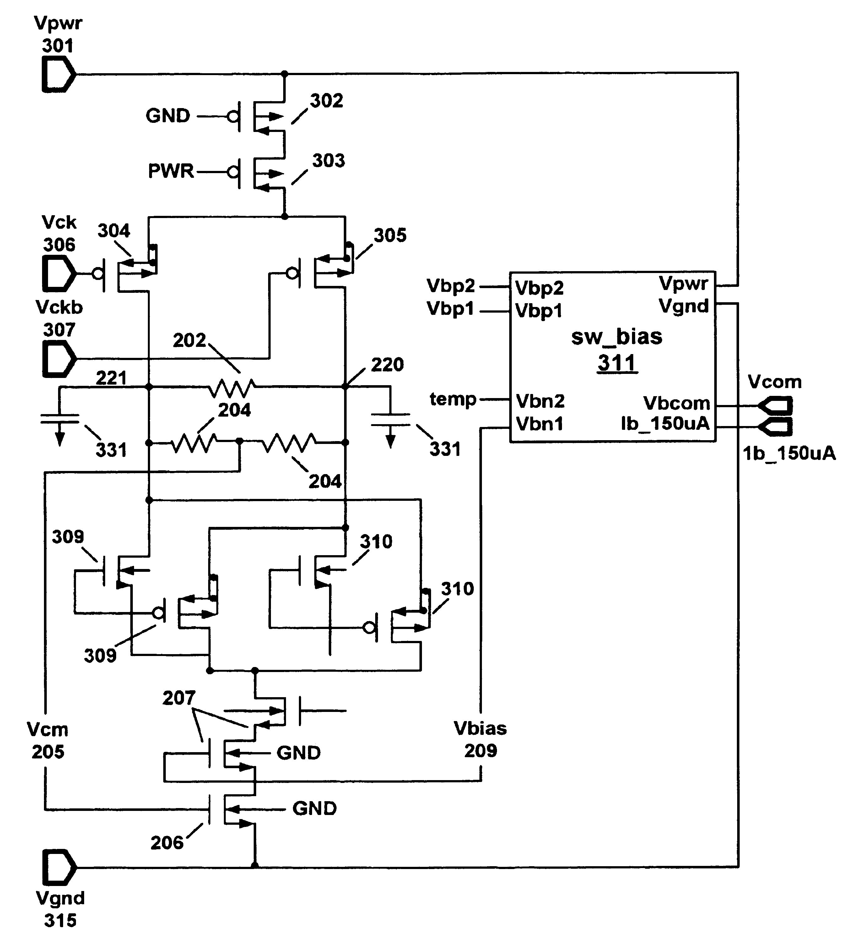
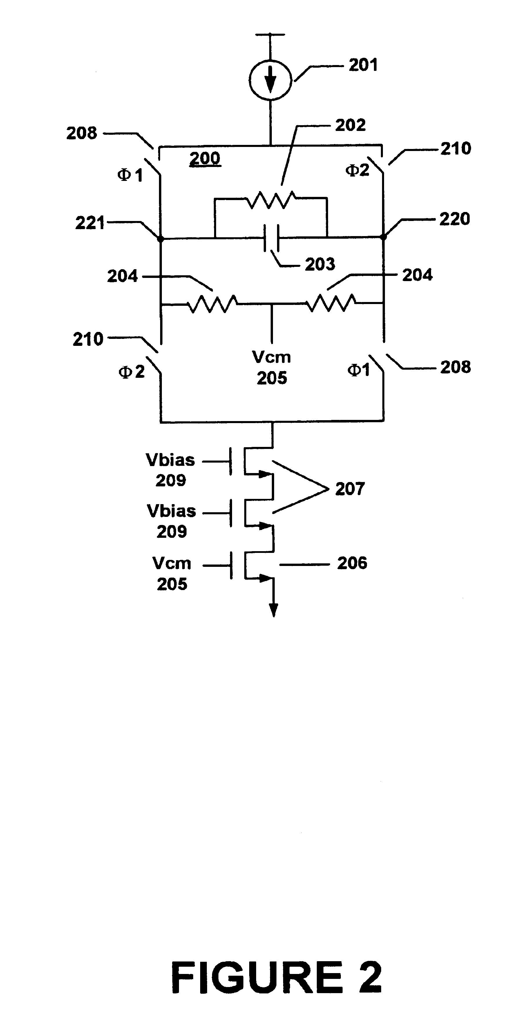
[0011]Embodiments of the present invention relate to a low voltage differential signal driver (LVDS) circuit which comprises a current source, logic controlled switches for controlling the driver's output, an electronic load circuit coupled across the circuit, and a common-mode resistor feedback circuit coupled across the circuit, in parallel with the RC load, for tuning the driver's output impedance. The driver is enabled to operate without op-amps and achieves optimum performance at 1.8V supply voltages.
[0012]Embodiments of the present invention can achieve signaling rates greater than 800 MHz by decreasing the output impedance during transition times. The circuit uses current mirrors and a common-mode feedback circuit to generate the proper LVDS signaling levels. No operational amplifiers (op-amps) are needed to control the current sources, which enables both optimum performance at 1.8V or lower supply voltages and design flexibility to manage speed versus power opportunities. Embodiments enable smaller RC-delays at the driver's output during signal transition than traditional LVDS drivers. This maximizes speed and stability for a given power and provides for significant flexibility because the designer can “program” the driver, by proper component selection, for a variety of common-mode differential signaling levels.
[0013]Specifically, in one embodiment, a 100 ohm, 5 pF, load creates a 50 pico-second RC delay that is managed by the driver circuit to meet desired operating speeds. Through the use of a common mode feedback circuit, embodiments of the present invention insert a small resistance in parallel with the LVDS load to decrease the effective LVDS output impedance and therefore decrease the delay inherent in the load. A resistance of 25-40 ohm, for instance enables the LVDS load induced to be decreased by approximately 70%. An impedance in this range still allows the driver to satisfy the TIA specified short circuit current specifications.
[0014]The resistance acts as a common-mode feedback circuit for the current sources. The current sources enable ample current to allow the LVDS signaling levels to be satisfied. This approach eliminates the need for operational amplifier control of the current sources. The common-mode feedback is adequate for controlling the current sources without the need of an active controller. This feature allows operation at lower power supply voltages.

Problems solved by technology

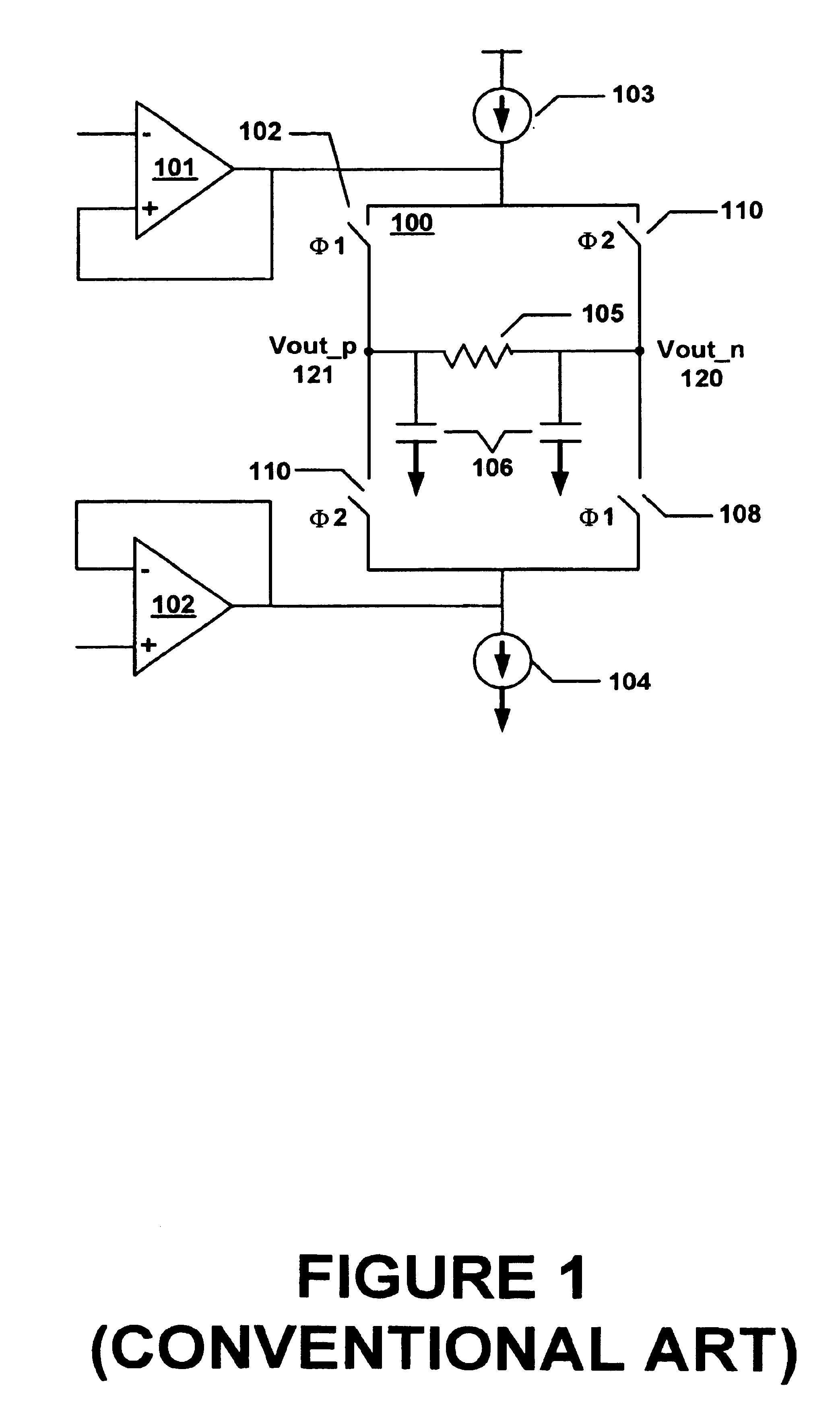
Moving high-bandwidth digital video data, for example, within modern consumer appliances and between them is a very challenging task.
The swing and common mode voltage are difficult to control and maintain over carriers.
This results in a significant RC delay that limits the maximum speed available for any given supply power.
With emerging chip technologies enabling sub-1.8V power supplies, building high-speed, TIA complaint, LVDS circuits becomes a challenge.
Traditional architectures, though, have not been able to take advantage of the emerging low power supply technologies.
By requiring op-amps to control the current sources, the flexibility or programmability of the traditional driver architecture has been limited to the input characteristics of the op-amps.
This does not enable most traditional LVDS drivers to be used at multiple power supply voltages and the tradeoff of power versus speed is not adjustable with existing architectures.

Method used


Image

  • Low voltage differential signal driver circuit and method
  • Low voltage differential signal driver circuit and method
  • Low voltage differential signal driver circuit and method

Examples


Embodiment Construction

[0021]Reference will now be made in detail to the preferred embodiments of the invention, examples of which are illustrated in the accompanying drawings. While the invention will be described in conjunction with the preferred embodiments, it will be understood that they are not intended to limit the invention to these embodiments. On the contrary, the invention is intended to cover alternatives, modifications and equivalents, which may be included within the spirit and scope of the invention as defined by the appended claims. Furthermore, in the following detailed description of the present invention, numerous specific details are set forth in order to provide a thorough understanding of the present invention. However, it should be understood by one of ordinary skill in the art that the present invention may be practiced without these specific details. In other instances, well-known methods, procedures, components, and circuits have not been described in detail so as not to unnecess...


PUM


Abstract

Embodiments of the present invention relate to a low voltage differential signal driver (LVDS) circuit which comprises a current source, logic controlled switches for controlling the driver's output, an electronic load circuit coupled across the circuit, and a common-mode resistor feedback circuit coupled across the circuit, in parallel with the RC load, for tuning the driver's impedance. The driver is enabled to operate without op-amps and achieves optimum performance at 1.8 v supply voltages.

Description

FIELD OF THE INVENTION[0001]Embodiments of the present invention relate to the field of low voltage semiconductor devices.BACKGROUND OF THE INVENTION[0002]Low-voltage differential signaling (LVDS) is a differential interconnectivity standard. It uses a low voltage swing of approximately 350 mV to communicate over a pair of traces on a PCB or cable.[0003]Electronic devices that require high speed communications, either internally or with other devices, use LVDS drivers extensively. Moving high-bandwidth digital video data, for example, within modern consumer appliances and between them is a very challenging task. This requires the speed that low power LVDS offers.[0004]Traditional LVDS drivers typically have architectures that require operational amplifiers (op-amps) to produce the voltages that control the current from two current sources and logic-controlled switches determine the direction of the current across a load. The direction of the current across the load determines the LV...

Claims


Application Information

Patent Timeline
IPC IPC(8): H03K19/094
CPCH04L25/028
Inventor ROPER, WESTONFENG, XIAOXIN
Owner TAIWAN SEMICON MFG CO LTD
Learn More