Bias controlled multi-spectral infrared photodetector and imager

a multi-spectral infrared and photodetector technology, applied in the field of infrared (ir) imaging, can solve the problems of non-uniformity in the fabrication process, the inability of conventional ir detector technology to adapt to the inability of conventional ir detector technology to meet the current demand for dual-band or multi-spectral detection, etc., to achieve the effect of convenient forming imag

Inactive Publication Date: 2005-05-24
LOCKHEED MARTIN CORP
View PDF53 Cites 17 Cited by
  • Summary
  • Abstract
  • Description
  • Claims
  • Application Information

AI Technical Summary

Problems solved by technology

Conventional IR detector technologies have proven difficult to adapt to this current demand for dual-band or multi-spectral detection.
The dual-band and multi-spectral HgCdTe photodetectors demonstrated to date have suffered significantly from both non-uniformity in the HgCdTe material and the fabrication process.
While dual-band and multi-spectral QWIP photodetectors do not place as stringent requirements upon the starting material, the fabrication process has similarly proven quite challenging.
Further, both IR detector technologies have suffered from reduced performance in dual-band or multi-spectral photodetectors in comparison to single band performance.

Method used


Image

  • Bias controlled multi-spectral infrared photodetector and imager
  • Bias controlled multi-spectral infrared photodetector and imager
  • Bias controlled multi-spectral infrared photodetector and imager

Examples


Embodiment Construction

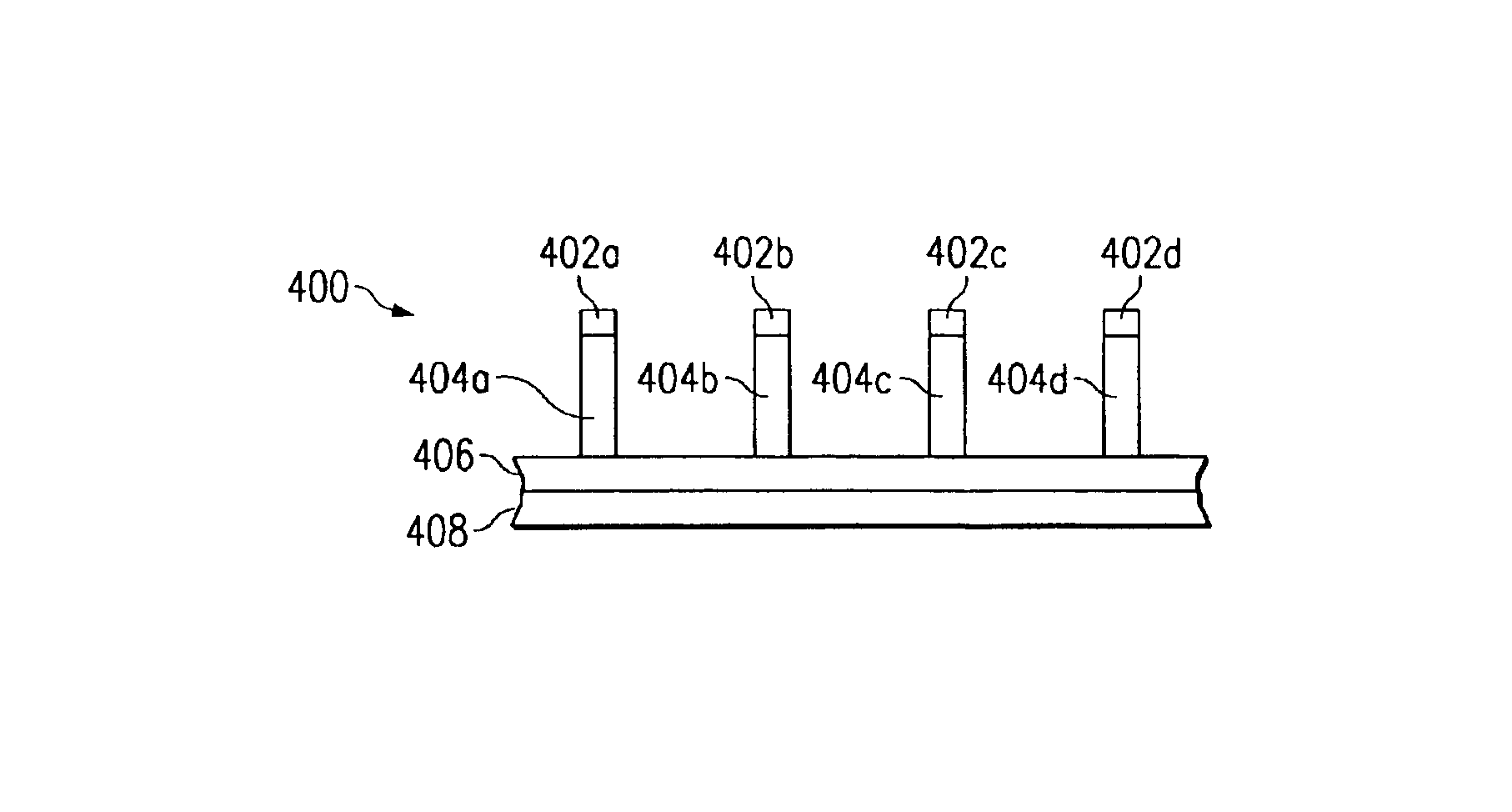
[0022]Various embodiments of the present invention are described in detail with reference to the drawings with corresponding elements having corresponding numbers throughout the drawings. While the following description will generally discuss a dual-band IR photodetector, altering the design of the IR absorbing layer can lead to absorption in three or more IR wavelength bands.

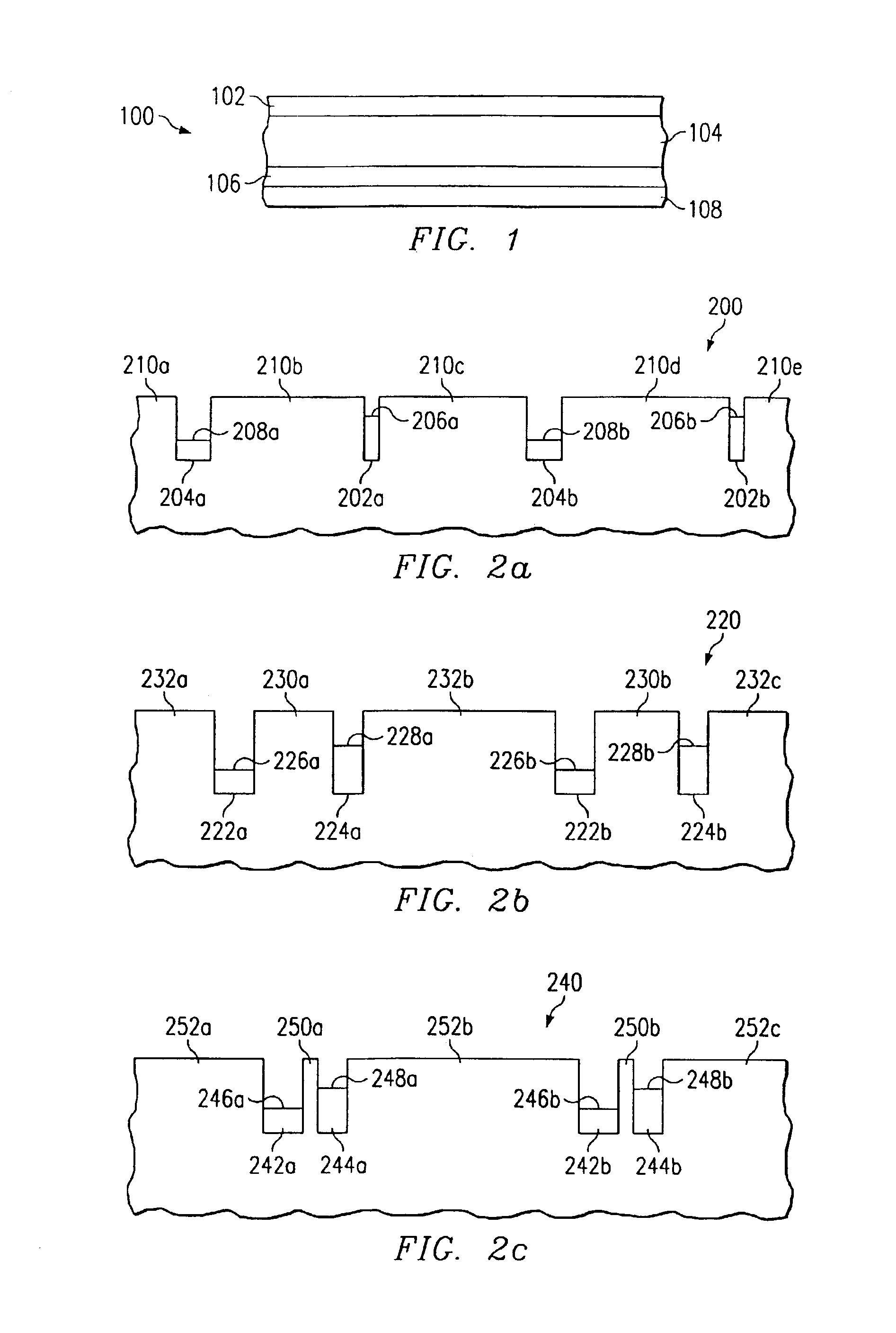
[0023]FIG. 1 is a cross-sectional view of the starting material 100 used in fabricating a dual-band IR photodetector in accordance with the two embodiments. The starting material 100 includes a series of laminae formed in succession. A top contact 102 is formed of doped semiconductor material. The top contact 102 is preferably heavily doped to reduce contact resistance and has a thickness of approximately 0.2 to 0.5 μm. An IR absorbing layer 104 is formed of semiconductor material that absorbs IR radiation in first and second IR wavelength bands. The IR absorbing layer 104 preferably has a thickness of between ...


PUM


Abstract

A multi-spectral photodetector for detecting two or more different bands of infrared radiation is described. The photodetector includes a diffractive resonant optical cavity that resonates at the two or more infrared radiation bands of interest. By detecting infrared radiation at two or more discrete applied biases and by generating a spectral response curve for the photodetector at each of these biases, the response to each of the individual bands of infrared radiation can be calculated. The response to each band of infrared radiation can be found by deconvolving the response at each bias. The photodetector finds many uses including military and medical imaging applications and can cover a broad portion of the infrared spectrum.

Description

BACKGROUND OF THE INVENTION[0001]In the field of infrared (IR) imaging, the current objective is to provide high pixel count imagers at low cost with high performance. InSb, HgCdTe and quantum well infrared photodetector (QWIP) technologies have demonstrated high performance large area imagers. Each of these technologies has various strengths and weaknesses. InSb photodetectors offer high performance, ease of fabrication and operation at wavelengths of less than 5 μm, but must be cooled to approximately 80 K. HgCdTe photodetectors can be designed to operate in the important long wavelength IR (LWIR) band corresponding to a wavelength range of 8 to 12 μm and the middle wavelength IR (MWIR) band corresponding to a wavelength range of 3 to 5 μm. HgCdTe photodetectors require very tight tolerances in material and fabrication uniformity, especially in the LWIR band, to ensure high performance. QWIP photodetectors have been demonstrated in both the MWIR and LWIR bands. Because of the matu...

Claims


Application Information

Patent Timeline
Patent Type & Authority Patents(United States)
IPC IPC(8): G01J5/10G01J5/60G01J3/26G01J3/36H01L31/101H01L31/103
CPCG01J3/26G01J3/36H01L31/1035G01J5/60H01L31/101G01J5/10
Inventor MITRA, PRADIP
Owner LOCKHEED MARTIN CORP
Why Eureka
Try Eureka