
Antiferroelectric liquid crystal display and method of driving the same

a liquid crystal display and antiferroelectric technology, applied in the direction of liquid crystal compositions, instruments, chemistry apparatus and processes, etc., can solve the problems of increasing the size and complexity of the liquid crystal display circuitry, increasing the manufacturing cost, and displaying image remains slightly visible on the screen

Inactive Publication Date: 2005-05-03
CITIZEN WATCH CO LTD
View PDF24 Cites 2 Cited by
  • Summary
  • Abstract
  • Description
  • Claims
  • Application Information

AI Technical Summary

Problems solved by technology

The conventional art driving method, however, has had the problem that after the same image pattern has been displayed for a long period of time, when a different image pattern is displayed on the screen, the previously displayed image remains slightly visible on the screen (this phenomenon is hereinafter called the “image sticking phenomenon”).
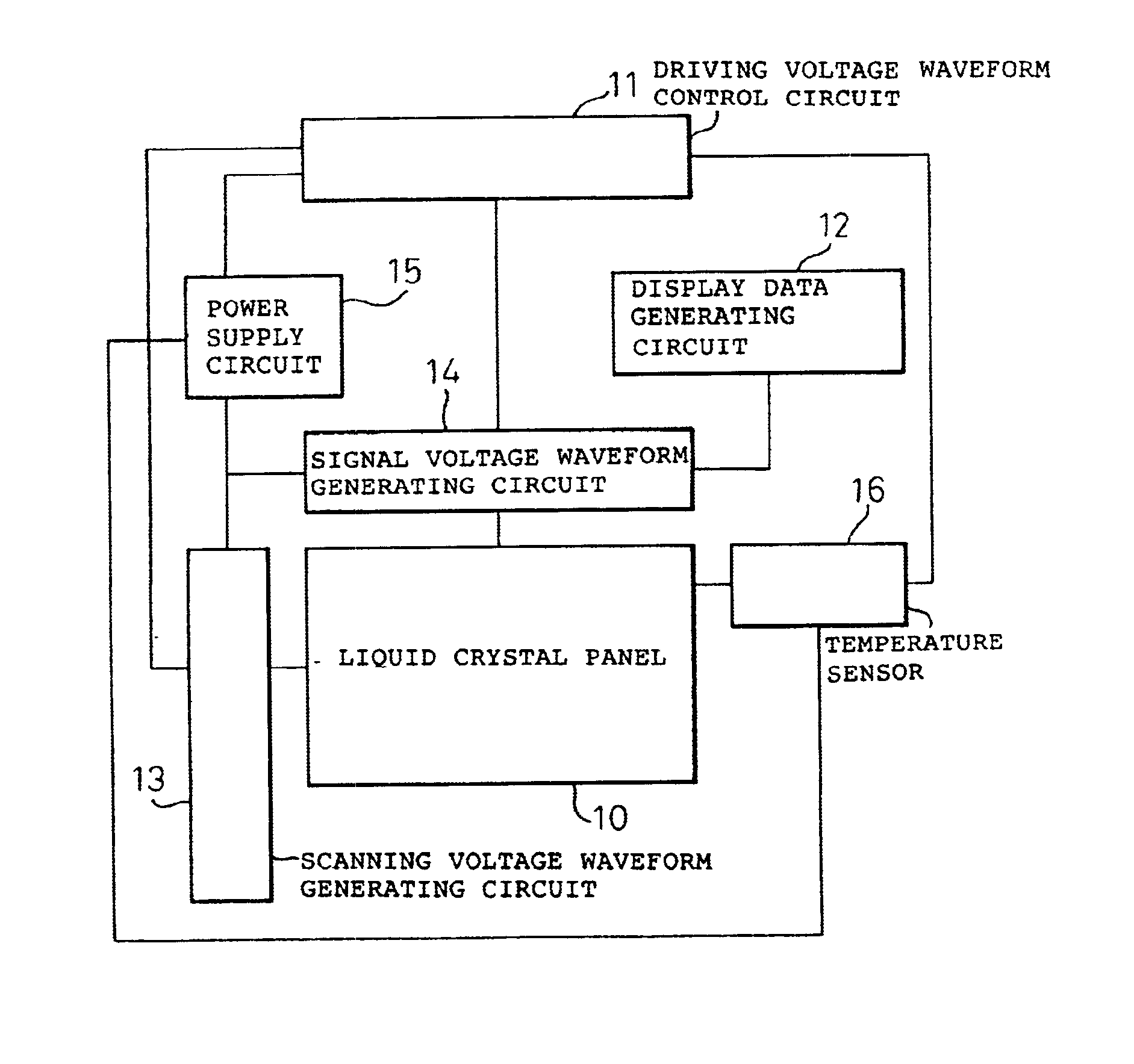
As a result, two circuits, i.e., the display driving circuit and the layer structure controlling voltage waveform circuit, must be provided for one liquid crystal display, which not only increases the size and complexity of the liquid crystal display circuitry but also leads to higher manufacturing costs.

Method used


Image

  • Antiferroelectric liquid crystal display and method of driving the same
  • Antiferroelectric liquid crystal display and method of driving the same
  • Antiferroelectric liquid crystal display and method of driving the same

Examples


Embodiment Construction

[0022]Embodiments of the present invention will be described in detail below with reference to the accompanying drawings.

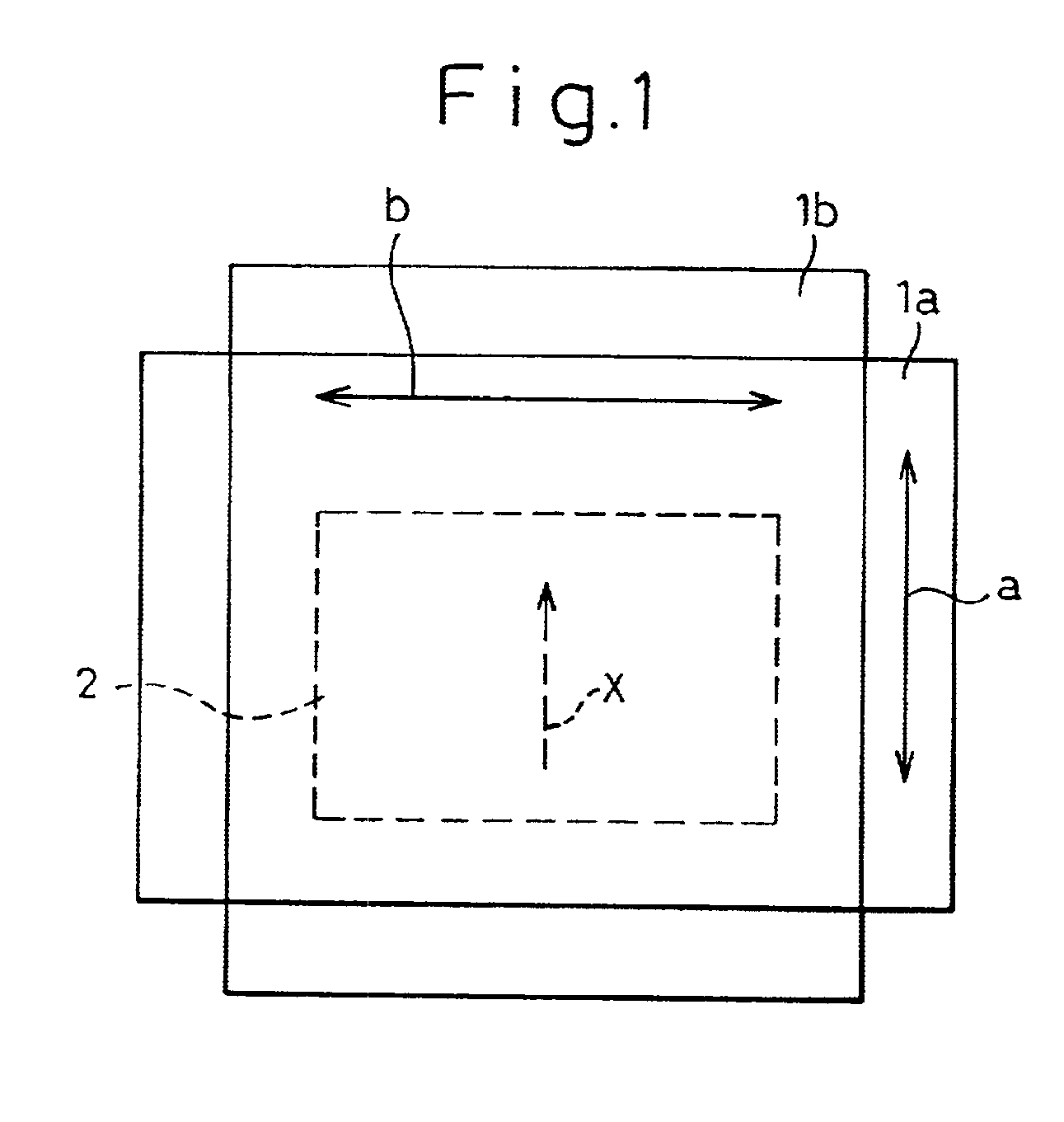
[0023]FIG. 1 is a diagram showing the arrangement of a liquid crystal device, when an antiferroelectric liquid crystal is used, as a display. Between polarizers 1a and 1b arranged in a crossed Nicol configuration is placed a liquid crystal cell 2 in such a manner that the average long axis direction X of molecules in the absence of an applied voltage is oriented substantially parallel to either the polarization axis, a, of the polarizer 1a or the polarization axis, b, of the polarizer 1b. Then, the liquid crystal cell is set up so that a black display is produced when no voltage is applied and a white display produced when a voltage is applied.

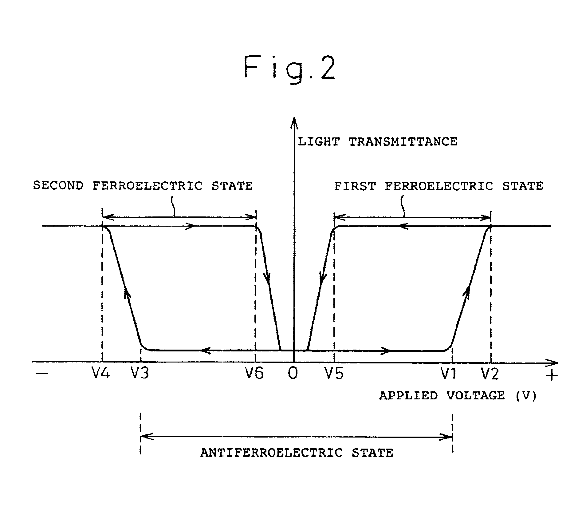
[0024]When the voltage is applied across the thus arranged liquid crystal device, its light transmittance varies with the applied voltage, describing a loop as plotted in the graph of FIG. 2. The voltage value at which the l...


PUM


Abstract

An antiferroelectric liquid crystal panel, having an antiferroelectric liquid crystal between a pair of substrates, which comprises a driving circuit adapted to output a layer structure controlling voltage waveform having a frequency of 1 Hz to 100 Hz and a voltage in the range of +10 V to +50 V or −10 V to −50 V, for an optional length of time.

Description

[0001]This is a continuation of application Ser. No .09 / 423,465, filed Nov. 9, 1999 which is a 371 of PCT / JP99 / 00959 filed Feb. 2, 1999, all of which are incorporated herein by referenceTECHNICAL FIELD[0002]The present invention relates to an antiferroelectric liquid crystal display, such as a liquid crystal display panel or a liquid crystal optical shutter array, having a liquid crystal layer of antiferroelectric liquid crystal, and a method of driving the same.BACKGROUND ART[0003]Liquid crystal panels using antiferroelectric liquid crystals have been researched extensively since it was reported in Japanese Patent Unexamined Publication No. 2-173724 by Nippondenso and Showa Shell Sekiyu that such liquid crystal panels provide wide viewing angles, are capable of fast response, and have good multiplexing characteristics.[0004]The conventional art driving method, however, has had the problem that after the same image pattern has been displayed for a long period of time, when a differe...

Claims


Application Information

Patent Timeline
IPC IPC(8): G09G3/36G02F1/133G02F1/13G02F1/141
CPCG09G3/3633G02F1/133382G02F2001/1412G09G2320/041G09G2310/06G02F1/1412G02F1/133
Inventor KONDOH, SHINYA
Owner CITIZEN WATCH CO LTD
Learn More