
N-Gate/N-Substrate or P-Gate/P-Substrate capacitor to characterize polysilicon gate depletion evaluation

a polysilicon gate and capacitor technology, applied in semiconductor/solid-state device testing/measurement, semiconductor devices, semiconductor/solid-state device details, etc., can solve the problems of time-consuming, labor-intensive, and expensive, and still be a complex, time-consuming, and expensive endeavor. , to achieve the effect of less complex process, less expensive, and faster

Inactive Publication Date: 2005-05-03
MONTEREY RES LLC
View PDF4 Cites 3 Cited by
  • Summary
  • Abstract
  • Description
  • Claims
  • Application Information

AI Technical Summary

Benefits of technology

[0010]Rather than using a traditional transistor structure to test the polysilicon gate depletion effects, the present invention uses a capacitor structure. The capacitor structure is a less complex process to construct than that of a transistor. As such, the present invention offers a faster, simpler, and less expensive method for determining the polysilicon gate depletion effects than that of the prior art.

Problems solved by technology

However, this is quite time consuming, labor intensive, and expensive.
Although fabricating a few test transistors is a more efficient way of evaluating the potentials of new fabrication processes, it can nonetheless be a complex, time-consuming, and expensive endeavor.

Method used


Image

  • N-Gate/N-Substrate or P-Gate/P-Substrate capacitor to characterize polysilicon gate depletion evaluation
  • N-Gate/N-Substrate or P-Gate/P-Substrate capacitor to characterize polysilicon gate depletion evaluation
  • N-Gate/N-Substrate or P-Gate/P-Substrate capacitor to characterize polysilicon gate depletion evaluation

Examples


Embodiment Construction

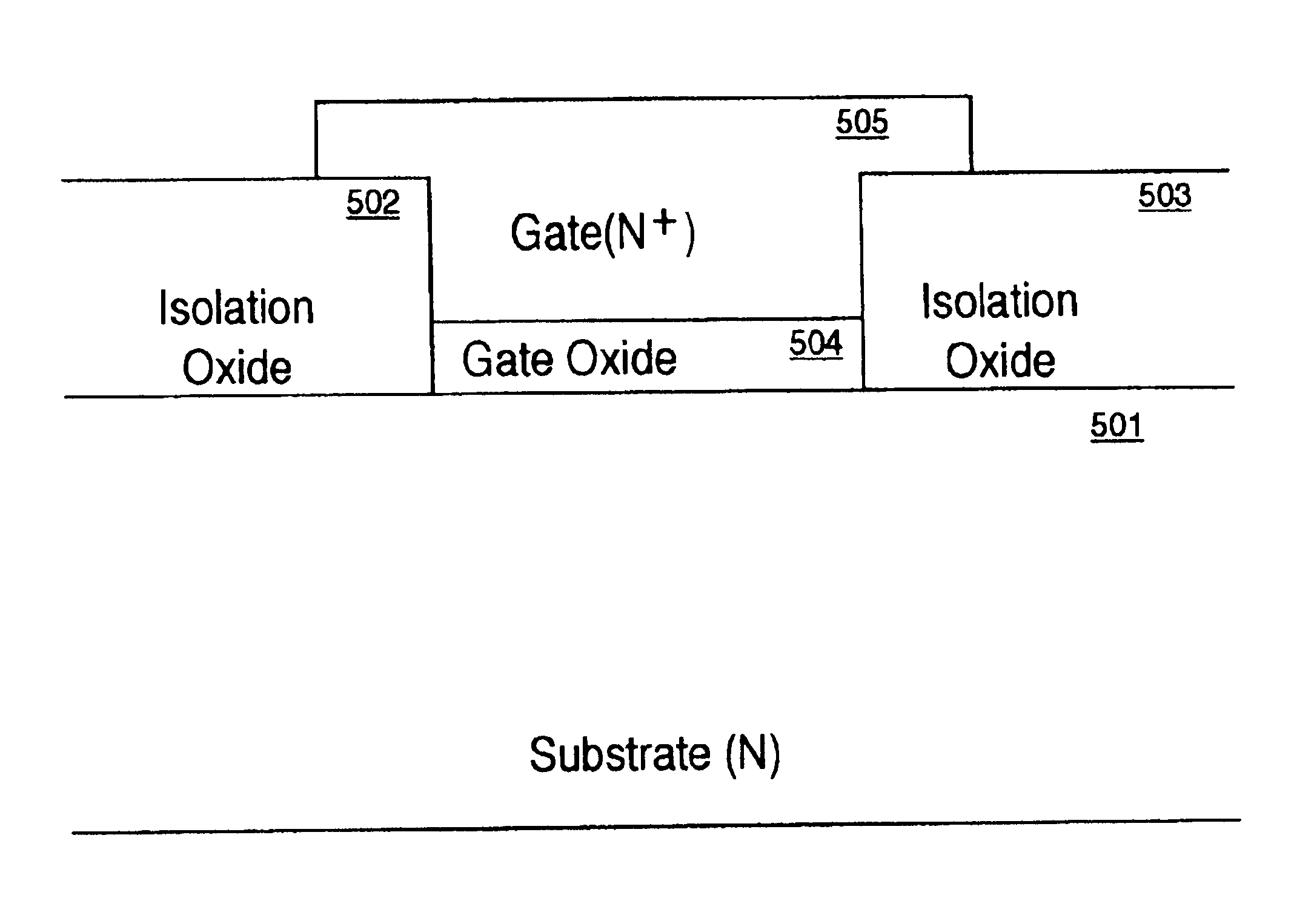
[0023]The present invention pertains to a short-loop method of utilizing N-Gate / N-Substrate (NN) and P-Gate / P-Substrate (PP) capacitors to evaluate polysilicon gate depletion. In the following detailed description of the present invention, numerous specific details are set forth in order to provide a thorough understanding of the present invention. However, it will be obvious to one skilled in the art that the present invention may be practiced without these specific details or by using alternate elements or methods. In other instances well known methods, procedures, components, and circuits have not been described in detail as not to unnecessarily obscure aspects of the present invention.

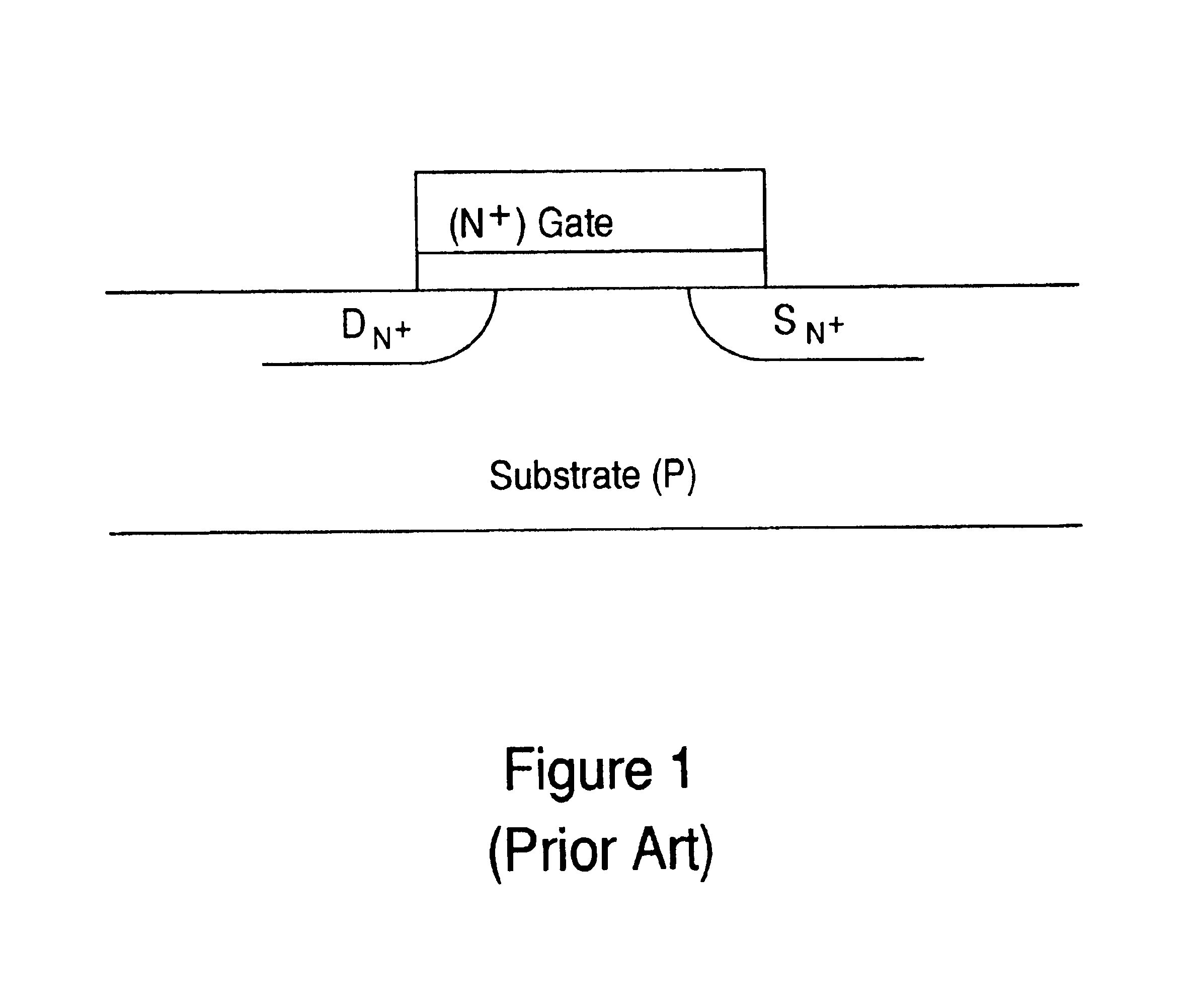
[0024]Before describing in detail the capacitors utilized in the present invention, it is beneficial to describe traditional capacitor structures. A traditional capacitor structure is shown in FIG. 3. It can be seen that this capacitor structure is comprised of a P-doped substrate 301, gate oxide 3...


PUM


Abstract

A capacitor structure for characterizing polysilicon gate depletion effects of a particular semiconductor fabrication process. In one embodiment, an N-Gate / N-Substrate capacitor is fabricated with the semiconductor fabrication process which is being evaluated for its polysilicon gate depletion effects. The N-gate of capacitor structure is driven to depletion while the N-substrate is simultaneously driven to accumulation. Capacitance-voltage measurements are taken. Based on these CV measurements, the polysilicon depletion effects are then obtained for that particular semiconductor fabrication process. In another embodiment, a P-Gate / P-Substrate capacitor is fabricated with the semiconductor fabrication process. The gate of the P-Gate / P-Substrate capacitor is driven to depletion while the substrate is simultaneously driven to accumulation. Based on the CV measurements performed on the P-Gate / P-Substrate capacitor, the polysilicon depletion effects can be obtained for that particular semiconductor fabrication process. In a third embodiment, a capacitor structure device is used to evaluate the polysilicon gate depletion effects of a semiconductor fabrication process. Different voltages are selectively applied to the gate of either an N-Gate / N-Substrate capacitor or a P-Gate / P-Substrate capacitor while its capacitance is measured. Based on the CV measurements, the polysilicon gate depletion effects for that particular semiconductor fabrication process is characterized.

Description

TECHNICAL FIELD[0001]The present invention relates to the field of semiconductor process evaluation. More specifically, the present invention pertains to a novel N Gate / N-Substrate or P Gate / P-Substrate capacitor to evaluate polysilicon gate depletion characteristics.BACKGROUND ART[0002]Rapid advances made in semiconductor fabrication processes enable the production of faster, more powerful, and less expensive semiconductor chips. Although the same principles for fabricating semiconductor chips are applied, there exist a wide array of different semiconductor fabrication processes. The particular fabrication process being utilized depends heavily on the type of chip being manufactured. For example, the semiconductor process for fabricating a memory chip is quite different than that of fabricating a microprocessor. Not only are there many different accepted processes for fabricating specific semiconductor chips, a particular process can be customized to meet the unique specifications ...

Claims


Application Information

Patent Timeline
Patent Type & Authority Patents(United States)
IPC IPC(8): H01L23/544
CPCH01L22/34H01L2924/0002H01L2924/00
Inventor WANG, ZHIGANGYANG, NIANHE, YUE-SONG
Owner MONTEREY RES LLC
Learn More