Method of molecular-scale pattern imprinting at surfaces

a technology of molecular scale and pattern, applied in the field of pattern imprinting, can solve the problems of not being able to produce large-scale patterns on the surface, not being able to make patterned masks with features smaller than tenths of a micron, and already suffering irreproducibility of masks with such small features

Inactive Publication Date: 2005-04-12
POLANYI JOHN C
View PDF23 Cites 8 Cited by
  • Summary
  • Abstract
  • Description
  • Claims
  • Application Information

AI Technical Summary

Benefits of technology

[0021]exposing said surface to an effective blocking agent subsequent to exposing said surface to said preselected molecules to militate against surface diffusion of said adsorbed molecules; and
[0022]forming an imprinted pattern covering less than every surface atom on said surface by irradiating the surface and the pattern

Problems solved by technology

It has not proved possible to make patterned masks having features smaller than tenths of a micron.
Moreover, masks with such small features already suffer from irreproducibility.
Such a method of marking a surface is not amenable to p

Method used


Image

  • Method of molecular-scale pattern imprinting at surfaces
  • Method of molecular-scale pattern imprinting at surfaces
  • Method of molecular-scale pattern imprinting at surfaces

Examples


Embodiment Construction

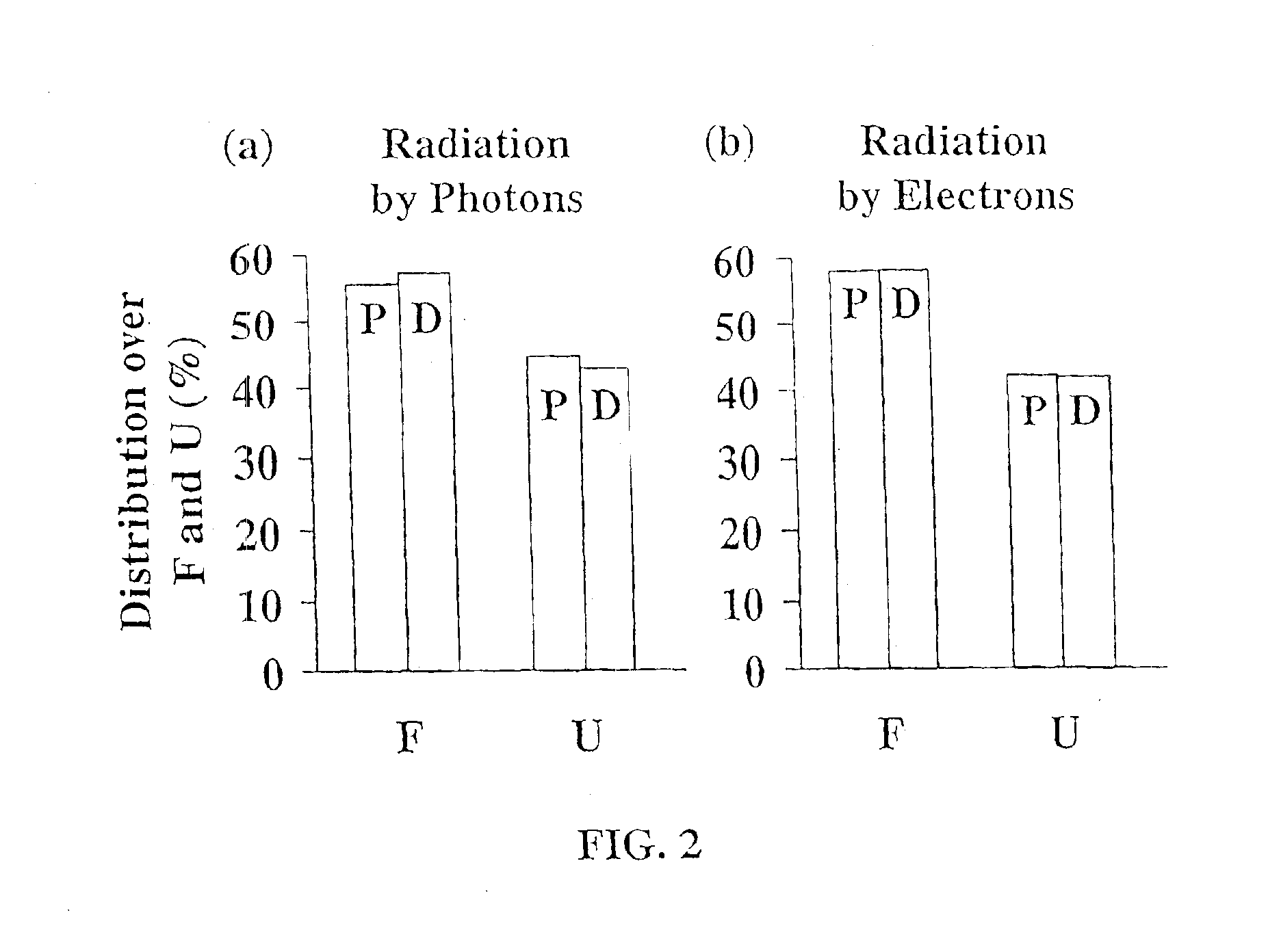
d to Si adatoms on F and U following irradiation by electrons.

[0051]FIG. 3(a) shows a bar graph showing the distribution of parent (ClBz) and daughter (Cl) species over adjacent atomic sites termed “middle atoms” designated (M) and corner atoms labeled (C) following irradiation by photons.

[0052]FIG. 3(b) shows a bar graph showing the distribution of parent (ClBz) and daughter (Cl) species over adjacent atomic sites termed “middle atoms” designated (M) and corner atoms labeled (C) following irradiation by electrons.

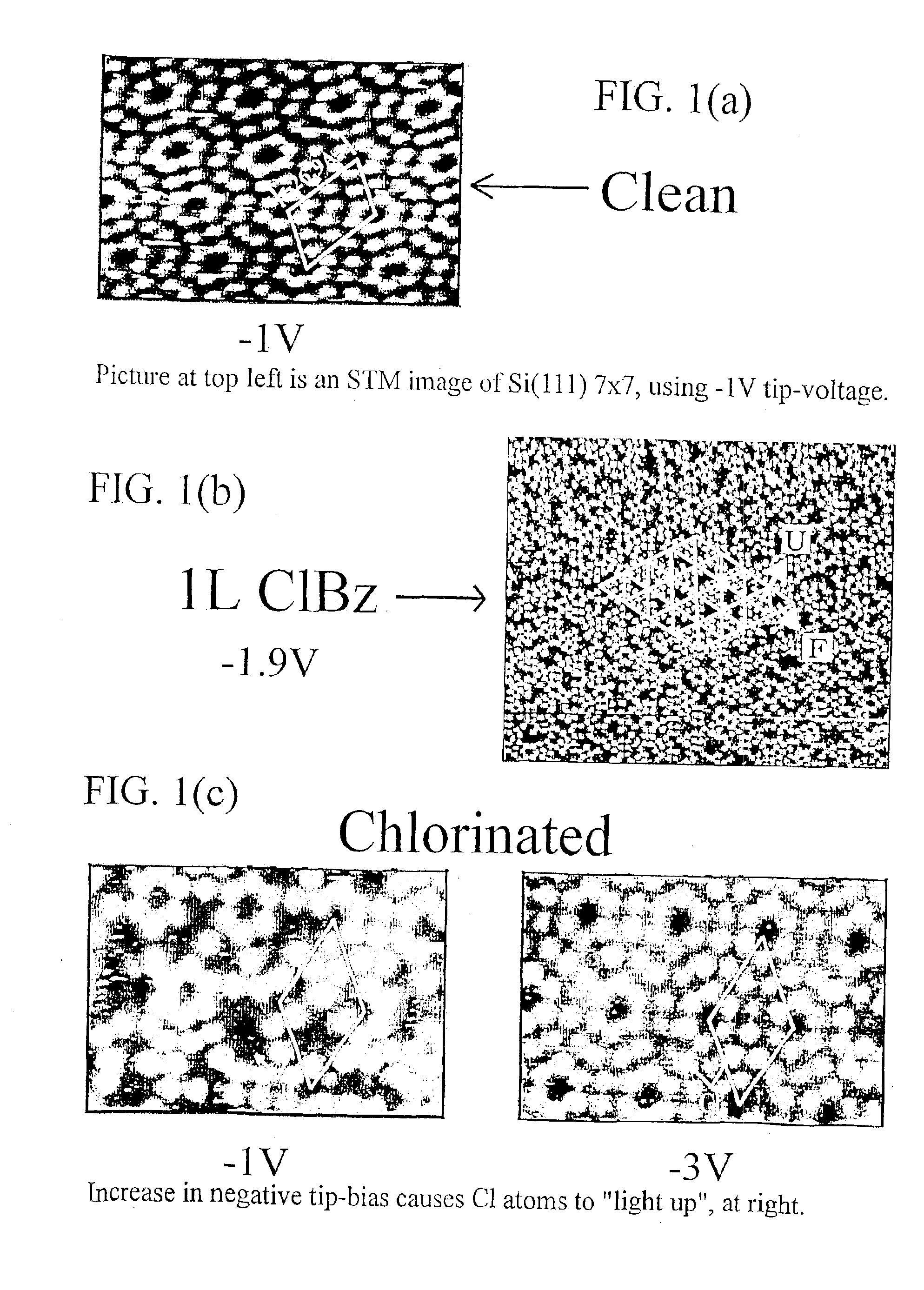
[0053]FIG. 4(a) shows a pattern of Cl atoms produced by irradiation using electrons from a scanning tunneling microscope (STM) tip of ClBz adsorbed on Si(111)7×7. The interrupted line of white spots was recorded with the tip at −3V, at which voltage Cl atoms ‘light up’ to form white spots. The −4V pulses at the STM tip were spaced at equal intervals of approximately 59 Å.

[0054]FIG. 4(b) shows a pattern of Cl atoms produced by irradiation using electrons from a scanning tun...


PUM

PropertyMeasurementUnit
Structureaaaaaaaaaa
Electrical conductoraaaaaaaaaa
Energyaaaaaaaaaa

Abstract

A method for mask-free molecular or atomic patterning of surfaces of reactive solids is disclosed. Molecules adsorb at surfaces in patterns, governed by the structure of the surface, the chemical nature of the adsorbate, and the adsorbate coverage at the surface. The surface is patterned and then imprinted with the pattern by inducing localized chemical reaction between adsorbate molecules and the surface of the solid, resulting in an imprint being formed in the vicinity of the adsorbate molecules. When the imprinted molecular patterns are conjugated chains containing π bonds along which electrical charge can flow the molecular patterns constitute molecular wires or the imprinted molecules constitute a molecular-scale device. The surface of the substrate can be doped by including n- or p-type dopants in the adsorbate molecules. These molecular wires are anchored to the substrate by using conjugated chains which can be chemically bound at intervals along the chains to the substrates.

Description

CROSS REFERENCE TO RELATED PATENT APPLICATION[0002]This patent application is a continuation-in-part patent application of U.S. patent application Ser. No. 09 / 573,683 filed on May 19, 2000 entitled METHOD OF MOLECULAR-SCALE PATTERN IMPRINTING AT SURFACES, which and which is incorporated herein by reference in its entirety.FIELD OF THE INVENTION[0003]The present invention relates to a method for pattern imprinting, on an atomic or molecular-scale, of the surface of a solid by inducing localized chemical reaction between adsorbate molecules and the surface of the solid.BACKGROUND OF THE INVENTION[0004]Progress in the hundred billion dollar semi-conductor industry depends, in part, on the ability to mark (i.e. write, dope or etch) a surface with small features at controlled separations. The current limit is the making of marks separated by a few tenths of a nanometer (commonly 0.3 microns, i.e. 3,000 A, which is roughly one thousand atoms separation). Patterns of these dimensions const...

Claims


Application Information

Patent Timeline
IPC IPC(8): C23C14/04G03F7/00H01L21/225H01L21/02
CPCB82Y10/00B82Y40/00H01L21/2254G03F7/0002C23C14/048
Inventor POLANYI, JOHN C.ROGERS, DUNCAN
Owner POLANYI JOHN C
Why Eureka
Try Eureka