Semiconductor device having an electrode overlaps a short carrier lifetime region
a technology of overlapping a carrier lifetime region and an electrode, which is applied in the direction of semiconductor devices, basic electric elements, electrical appliances, etc., can solve the problem that countermeasures are not fully effective in and achieve the effect of improving reverse-recovery withstanding capability
- Summary
- Abstract
- Description
- Claims
- Application Information
AI Technical Summary
Benefits of technology
Problems solved by technology
Method used
Image

Examples
first embodiment
of the Invention
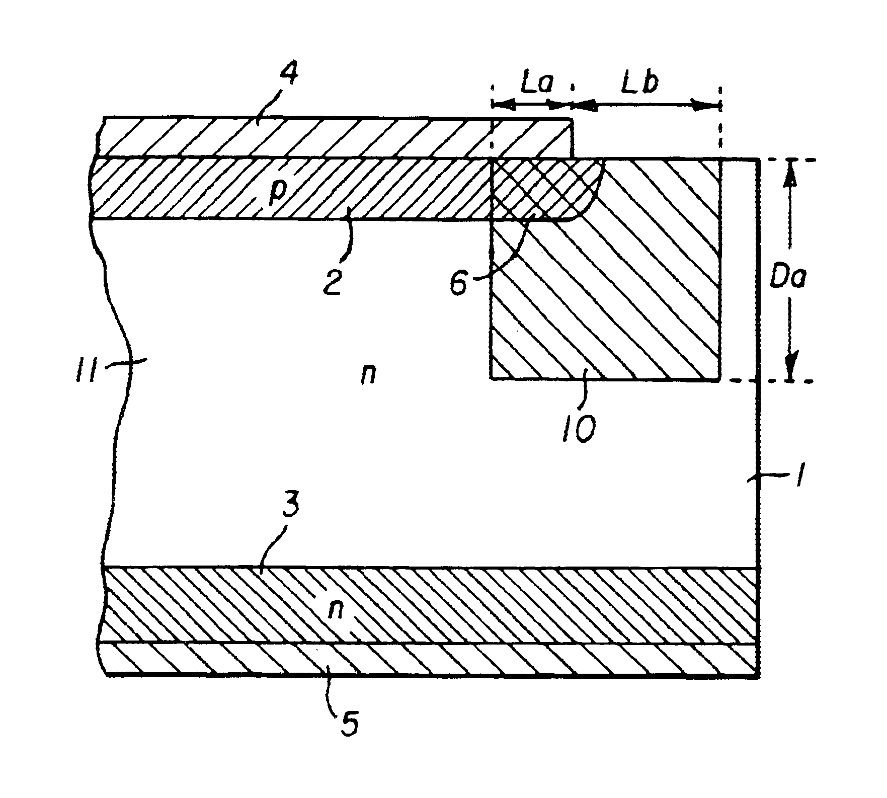
The first embodiment of the invention will be explained with reference to FIGS. 1 through 6. Referring to FIG. 1, an n-type semiconductor substrate 1 is formed as a lightly doped semiconductor layer. A p-type anode layer 2 is formed as a heavily doped conductive region selectively on a first major surface of n-type semiconductor substrate 1. An n-type cathode layer 3 is formed as another heavily doped conductive region on a second major surface of n-type semiconductor substrate 1.
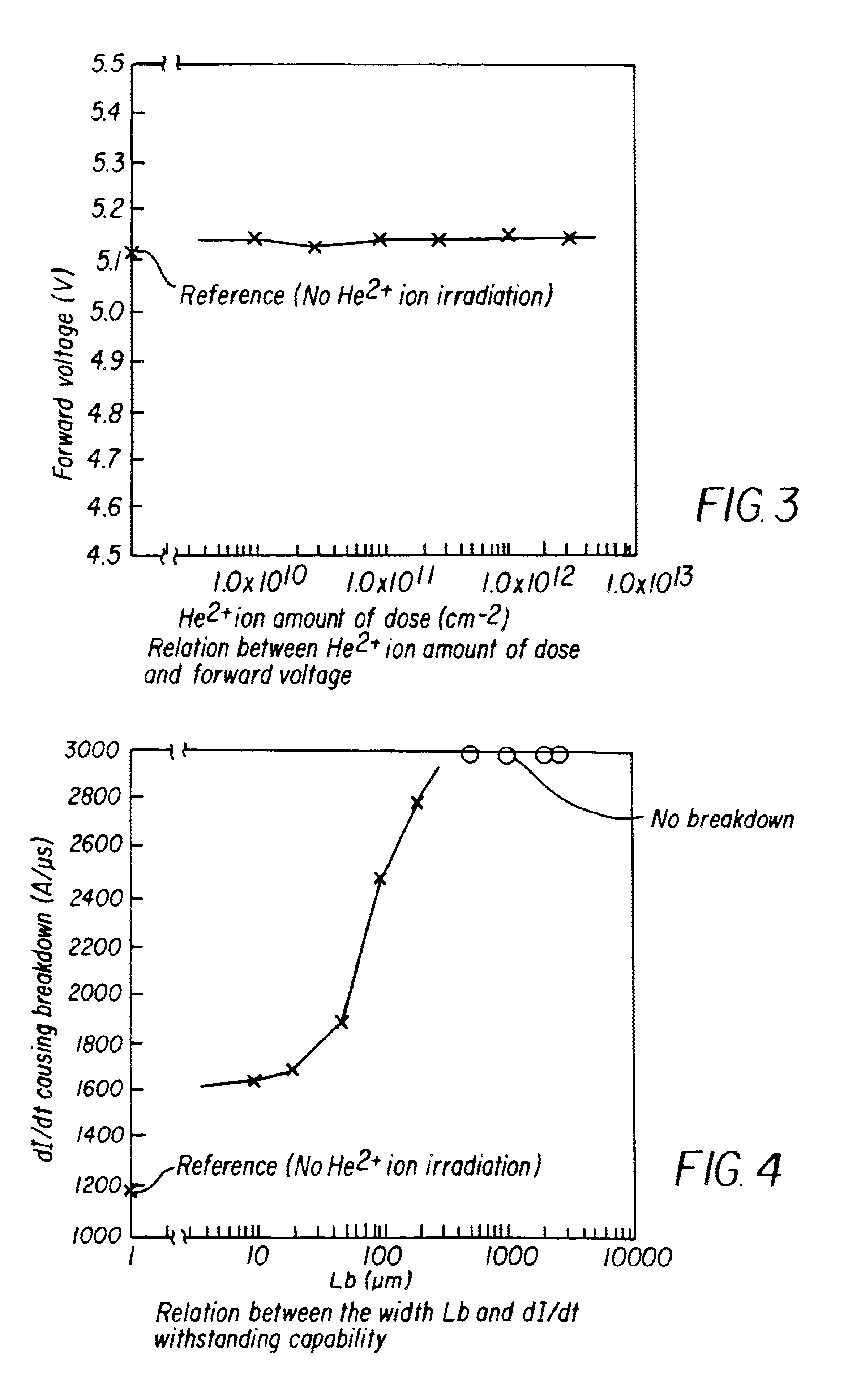
A metal anode electrode 4 is formed on p-type anode layer 2. The edge area of anode electrode 4 is spaced apart for 10 micrometers inward from the edge area of type anode layer 2. A cathode electrode 5 is formed on the entire surface of n-type cathode layer 3.
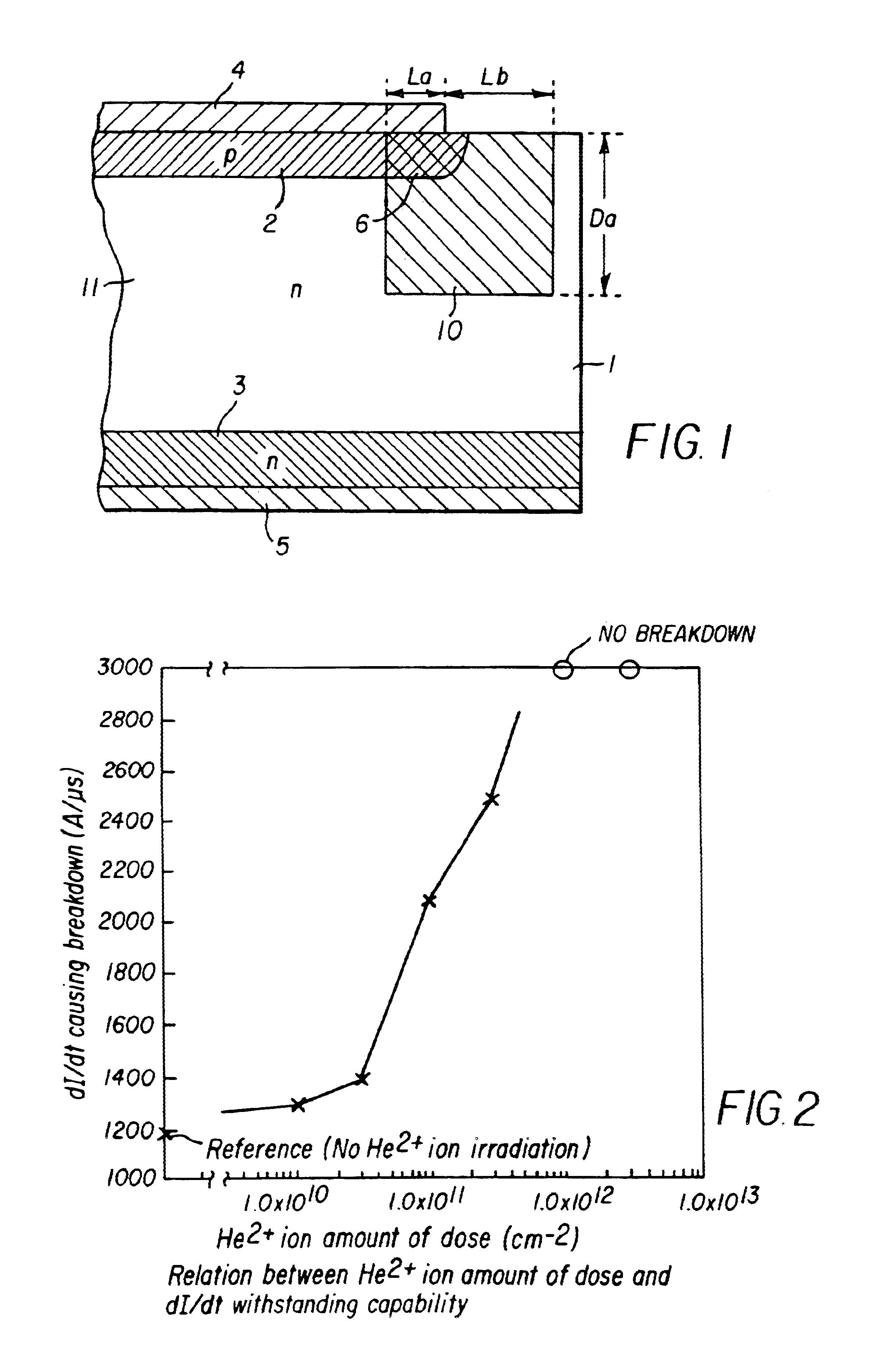
A first carrier lifetime region 10 and a second carrier lifetime region 11 are formed in n-type semiconductor substrate 1, so that the diode according to the first embodiment may exhibit two carrier lifetimes. First carrier lifetime reg...
second embodiment
of the Invention
A second preferred embodiment of the invention will now be explained with reference to FIGS. 7 through 13. In FIGS. 7 through 13, the same reference numerals as used in FIGS. 1 through 6 are used to identify the same constituent elements.
FIG. 7 is a cross sectional view of a p-i-n diode according to this second embodiment of the invention that includes a first carrier lifetime region 10 (in which the carrier lifetime is short) in a location of the semiconductor substrate different from the location of the first carrier lifetime region shown in FIG. 1.
In the diode structure shown in FIG. 7, the edge area of a p-type anode layer 2 and the edge area of an anode electrode 4 are spaced apart about 300 micrometers from each other. First carrier lifetime region 10 (in which the carrier lifetime is short) is formed in such a way that first carrier lifetime region 10 does not include the edge area X of p-type anode layer (p-type well region) 2; extends across the edge area of...
third embodiment
of the Invention
A third preferred embodiment of the invention will now be described with reference to FIG. 14, which shows a cross sectional view of a p-i-n diode. Referring to FIG. 14, the diode according to this third embodiment includes a non-contact region 15 between two separate p-type anode regions 2 and 2.
A first carrier lifetime region 10 (in which the carrier lifetime is short) is formed in the same way as in the diode of FIG. 1, such that first carrier lifetime region 10 extends across the edge area X of anode electrode 4 and includes boundary area 6, where p-type anode layer 2 and lightly doped semiconductor layer 11 contact each other. By forming first carrier lifetime region 10 (in which the carrier lifetime is short) in such a configuration that first carrier lifetime region 10 extends across the edge area X of anode electrode 4 and includes the boundary area 6, current localization in the vicinity of the electrode edge area is prevented from occurring. Further, the re...
PUM
 Abstract
Description
Claims
Application Information
 - R&D
- Intellectual Property
- Life Sciences
- Materials
- Tech Scout
- Unparalleled Data Quality
- Higher Quality Content
- 60% Fewer Hallucinations
Browse by: Latest US Patents, China's latest patents, Technical Efficacy Thesaurus, Application Domain, Technology Topic, Popular Technical Reports.
© 2025 PatSnap. All rights reserved.Legal|Privacy policy|Modern Slavery Act Transparency Statement|Sitemap|About US| Contact US: help@patsnap.com