Addition circuit for digital data with a delayed saturation operation for the most significant data bits
- Summary
- Abstract
- Description
- Claims
- Application Information
AI Technical Summary
Benefits of technology
Problems solved by technology
Method used
Image
Examples
Embodiment Construction
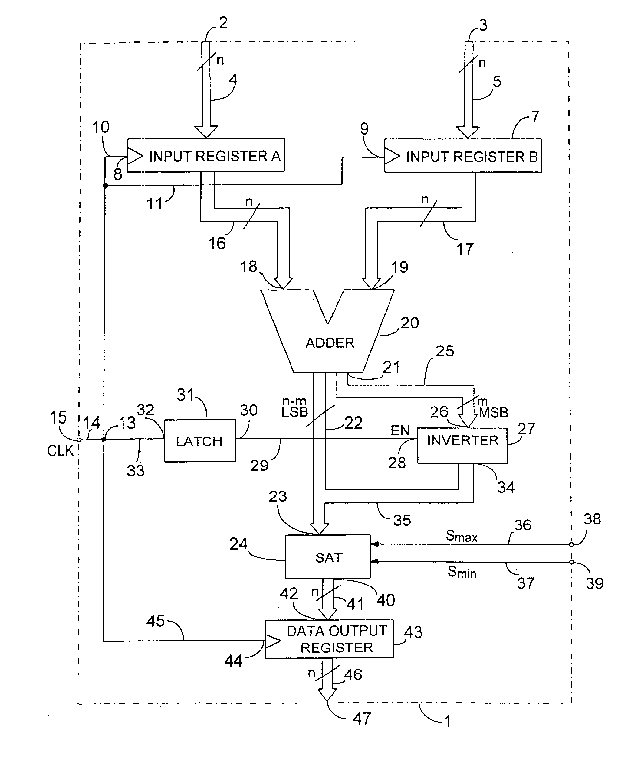
As FIG. 3 reveals, the addition circuit 1 according to the invention has a first data input 2 and a second data input 3 for applying digital input data values. The present input data values are written to input registers 6, 7, n bits wide in each case, via n parallel data lines 4, 5 for buffer storage. The input registers 6, 7 have in each case a clock signal input 8, 9. The clock signal inputs 8, 9 of the two input registers 6, 7 are connected via clock lines 10, 11, 12 to a clock-signal branching node 13 of the addition circuit 1. The clock-signal branching node 13 is connected via an internal clock line 14 to a clock-signal input 15 of the addition circuit 1. The data outputs of the input registers 6, 7 are connected via n parallel data lines 16, 17 to data inputs 18, 19 of a digital adder 20. The digital adder 20 is preferably composed of full-adder components. The digital adder 20 adds the two digital input data values present at the digital data inputs 18, 19 and delivers a su...
PUM
 Abstract
Description
Claims
Application Information
 - R&D
- Intellectual Property
- Life Sciences
- Materials
- Tech Scout
- Unparalleled Data Quality
- Higher Quality Content
- 60% Fewer Hallucinations
Browse by: Latest US Patents, China's latest patents, Technical Efficacy Thesaurus, Application Domain, Technology Topic, Popular Technical Reports.
© 2025 PatSnap. All rights reserved.Legal|Privacy policy|Modern Slavery Act Transparency Statement|Sitemap|About US| Contact US: help@patsnap.com


