Cu film deposition equipment of semiconductor device

a technology of cu film and equipment, applied in the direction of semiconductor/solid-state device details, chemical vapor deposition coating, coating, etc., can solve the problems of major cost disadvantage, cumbersome commercial use, and the like, and achieve the effects of controlling the texture of the cu thin film, enhancing adhesion, and enhancing adhesion

Inactive Publication Date: 2005-02-15
SK HYNIX INC
View PDF5 Cites 0 Cited by
  • Summary
  • Abstract
  • Description
  • Claims
  • Application Information

AI Technical Summary

Benefits of technology

An object of the present invention is to provide Cu film deposition equipment for a semiconductor device that enables CE and plasma treatment and at the same time removes residue produced from the surface after the deposition of a Cu thin film through plasma treatment, thereby increasing Cu thin film deposition speed and lowering the production cost.
These and other objects are further accomplished by Cu film deposition equipment for a semiconductor device comprising a load lock carrying out intermediate steps before and after a plurality of wafer processes; an aligner carrying out an alignment process, the alignment process ensuring a wafer reaches a desired position; a de-gas chamber removing residue produced on a surface of the wafer; a first feeding chamber provided with a robot, the feeding chamber positioning the wafer in and out of chambers for the wafer processes; a pre-cleaning chamber cleaning an inside and an outside of a pattern using plasma on the wafer fed by the first feeding chamber; a barrier metal deposition chamber depositing a barrier metal on the pre-cleaned wafer; a PVD Cu deposition chamber depositing flash Cu on the barrier metal to enhance adhesion of a CVD Cu; a second feeding chamber feeding the wafer deposited with flash Cu; a third feeding chamber positioning the wafer fed by the second feeding chamber in and out of chambers of the wafer processes; a CE treatment chamber processing an equal Chemical Enhancer (CE) treatment on an entire surface of the wafer positioned by the third feeding chamber; a plasma treatment chamber processing a plasma treatment on an entire surface of the wafer treated with CE to form an equal super-filling; a CECVD Cu deposition chamber depositing a Cu thin film on the entire surface of the wafer processed by particle filling; and an in-situ annealing chamber enhancing adhesion and controlling texture of the Cu thin film.
These and other objects are further accomplished by Cu film deposition equipment for a semiconductor device comprising a load lock carrying out intermediate steps before and after a plurality of wafer processes; an aligner carrying out an alignment process, the alignment process ensuring a wafer reaches a desired position; a de-gas chamber removing residue produced on a surface of the wafer; a first feeding chamber provided with a robot, the feeding chamber positioning the wafer in and out of chambers for the wafer processes; a pre-cleaning chamber cleaning an inside and an outside of a pattern using plasma on the wafer fed by the first feeding chamber; a barrier metal deposition chamber depositing a barrier metal on the pre-cleaned wafer; a PVD Cu deposition chamber depositing flash Cu on the barrier metal to enhance adhesion of a CVD Cu; a second feeding chamber feeding the wafer deposited with flash Cu; a third feeding chamber positioning the wafer fed by the second feeding chamber in and out of chambers of the wafer processes; a first CECVD Cu deposition chamber processing a first particle filling step on an entire surface of the wafer positioned by the third feeding chamber; a plasma treatment chamber processing a plasma treatment on the entire surface of the wafer processed by the first particle filling step; a second CECVD Cu deposition chamber processing a second particle filling step on the entire surface of the wafer treated with plasma; a CVD Cu deposition chamber depositing a Cu thin film on the entire surface of the wafer processed by the first and second particle filling steps; and an in-situ annealing chamber enhancing adhesion and controlling texture of the Cu thin film.
These and other objects are further accomplished by Cu film deposition equipment for a semiconductor device comprising a load lock carrying out intermediate steps before and after a plurality of wafer processes; an aligner carrying out an alignment process, the alignment process ensuring a wafer reaches a desired position; a de-gas chamber removing residue produced on a surface of the wafer; a first feeding chamber provided with a robot, the feeding chamber positioning the wafer in and out of chambers for the wafer processes; a pre-cleaning chamber cleaning an inside and an outside of a pattern using plasma on the wafer fed by the first feeding chamber; a barrier metal deposition chamber depositing a barrier metal on the pre-cleaned wafer; a first plasma treatment chamber processing a plasma treatment on an entire surface of the wafer where barrier metal is formed; a second feeding chamber feeding the wafer treated with plasma; a third feeding chamber positioning the wafer fed by the second feeding chamber in and out of chambers for the wafer processes; a CE treatment chamber processing an equal Chemical Enhancer (CE) treatment on the entire surface of the wafer put in by the third feeding chamber; a second plasma treatment chamber processing a plasma treatment on the entire surface of the wafer treated with CE to form an equal super-filling; a CECVD Cu deposition chamber depositing a Cu thin film on the entire surface of the wafer processed by particle filling; and an in-situ annealing chamber enhancing adhesion and controlling texture of the Cu thin film.
These and other objects are further accomplished by Cu film deposition equipment for a semiconductor device comprising a load lock carrying out intermediate steps before and after a plurality of wafer processes; an aligner carrying out an alignment process, the alignment process ensuring a wafer reaches a desired position; a de-gas chamber removing residue produced on a surface of the wafer; a first feeding chamber provided with a robot, the feeding chamber positioning the wafer in and out of chambers for the wafer processes; a pre-cleaning chamber cleaning an inside and an outside of a pattern using plasma on the wafer fed by the first feeding chamber; a barrier metal deposition chamber depositing a barrier metal on the pre-cleaned wafer; a first plasma treatment chamber processing a plasma treatment on an entire surface of the wafer where barrier metal is formed; a second feeding chamber feeding the wafer treated with plasma; a third feeding chamber positioning the wafer fed by the second feeding chamber in and out of chambers for the wafer processes; a first CECVD Cu deposition chamber processing a first particle filling step on the entire surface of the wafer put in by the third feeding chamber; a second plasma treatment chamber processing a plasma treatment on the entire surface of the wafer processed by the first particle filling step; a second CECVD Cu deposition chamber processing a second particle filling step on the entire surface of the wafer treated with plasma; a CVD Cu deposition chamber depositing a Cu thin film on the entire surface of the wafer processed by the first and second particle filling steps; and an in-situ annealing chamber enhancing adhesion and controlling texture of the Cu thin film.

Problems solved by technology

However, the related art Cu film deposition equipment suffers from the following disadvantages.
In the case where a Cu thin film is deposited by the MOCVD process, a problem arises in that it is cumbersome in commercial use due to its relatively low deposition speed.
Additionally, further problems arise in that adhesion and texture quality are less than desirable, thereby resulting in a major cost disadvantage as compared to the electroplating process.
However, a problem arises in that no CVD equipment cluster is provided in which an in-situ process is carried out after the use of a barrier deposition and a catalyst enabling plasma treatment.

Method used


Image

  • Cu film deposition equipment of semiconductor device
  • Cu film deposition equipment of semiconductor device
  • Cu film deposition equipment of semiconductor device

Examples


first embodiment

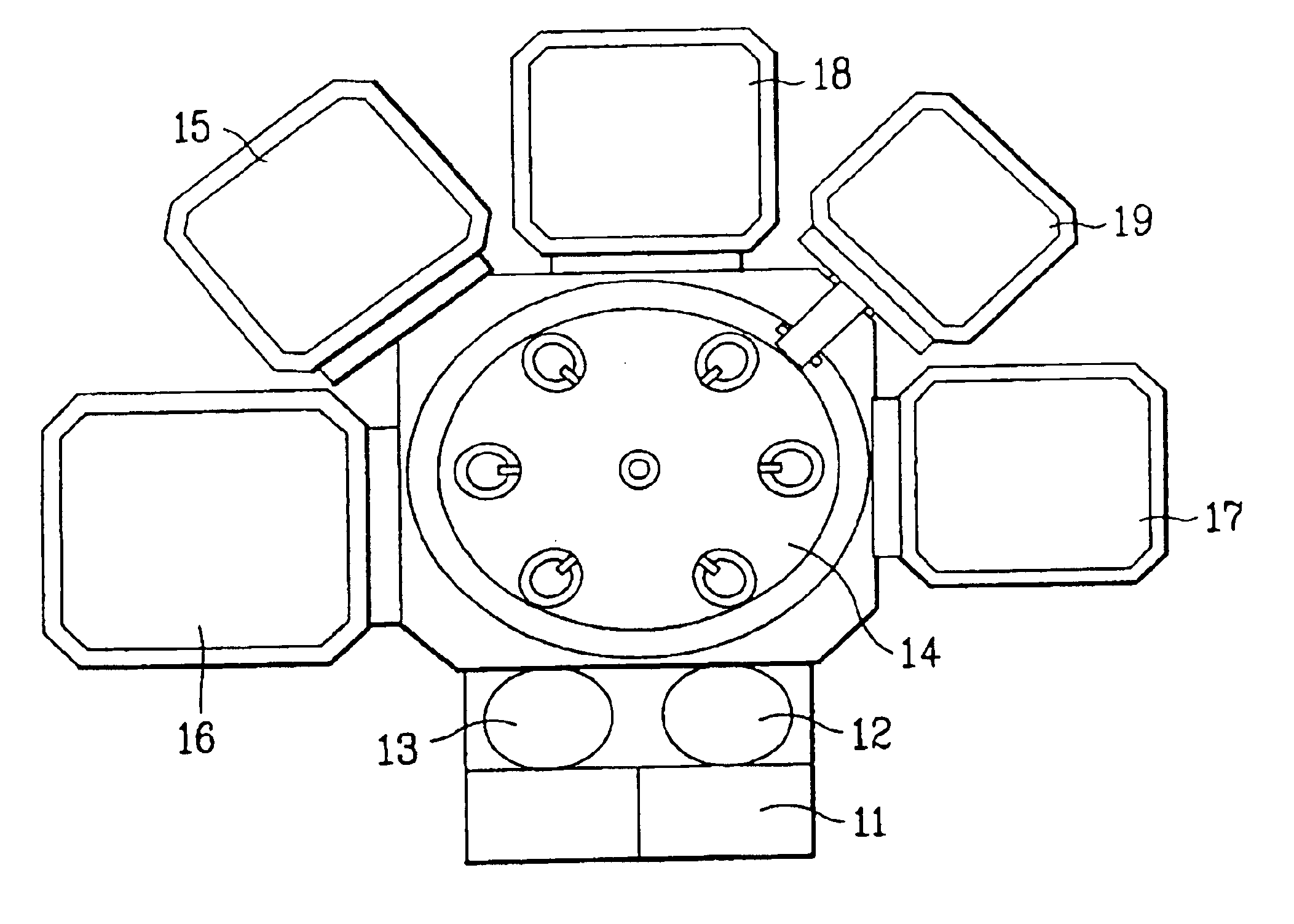
FIG. 1 is a plan view of a Cu film deposition equipment structure according to a first embodiment of the present invention. As shown in FIG. 1, the Cu film deposition equipment of the present invention includes a load lock 11 carrying out the steps before and after wafer (not shown) processes, an aligner 12 carrying out alignment so that the wafer reaches a desired position, and a de-gas chamber 13 removing residue such as gas produced on a surface of the wafer. A feeding chamber 14 provided with a robot moves the wafer in / out of each chamber.

The Cu film deposition equipment also includes a pre-cleaning chamber 15 cleaning the inside and the outside of a pattern using plasma on the wafer fed by the feeding chamber 14, a barrier metal deposition chamber 16 depositing barrier metal on the pre-cleaned wafer, an adhesion glue layer (AGL) flash Cu deposition chamber 17 depositing flash Cu as an AGL on the barrier metal to enhance adhesion of the Cu thin film before depositing the film, a...

second embodiment

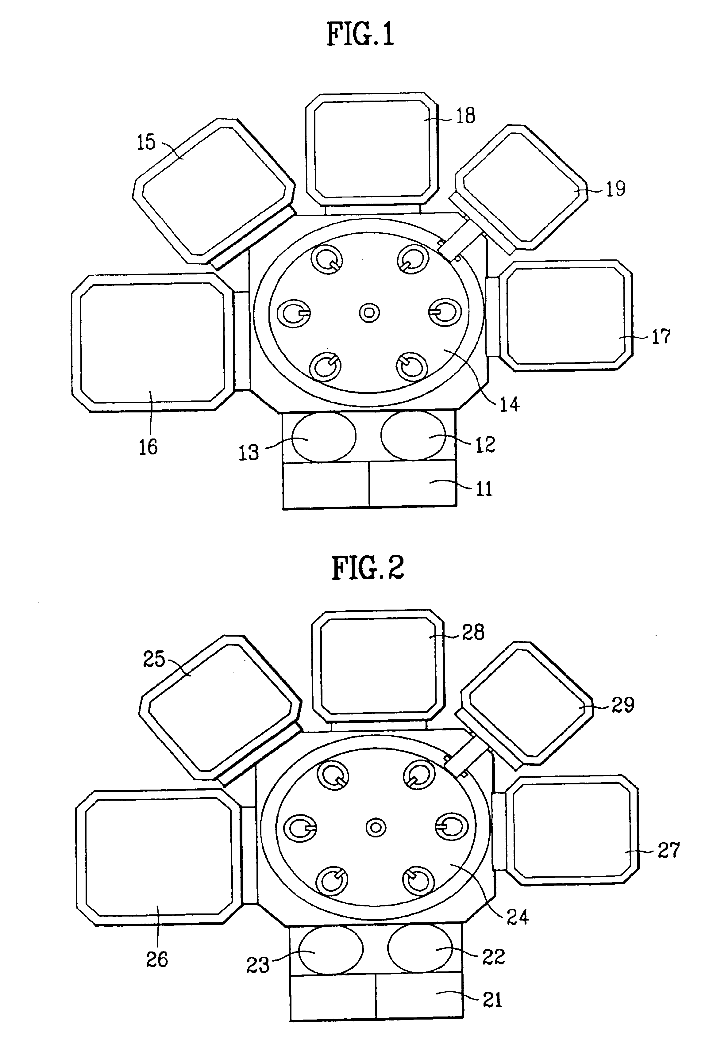
FIG. 2 is a plan view of a Cu film deposition equipment structure according to a second embodiment of the present invention. As shown in FIG. 2, the Cu film deposition equipment of the present invention includes a load lock 21 carrying out the steps before and after wafer (not shown) processes, an aligner 22 carrying out alignment so that the wafer reaches a desired position, and a de-gas and in-situ annealing chamber 23 removing residue such as gas produced on a surface of the wafer and processing in-situ annealing to enhance adhesion of a Cu thin film deposited and to control a texture of the Cu thin film. A feeding chamber 24 provided with a robot places the wafer in / out of each chamber.

The Cu film deposition equipment also includes a pre-cleaning chamber 25 cleaning the inside and the outside of a pattern using plasma on the wafer fed by the feeding chamber 24, a barrier metal deposition chamber 26 depositing barrier metal on the pre-cleaned wafer by PVD, CVD, or ALD processes, ...

third embodiment

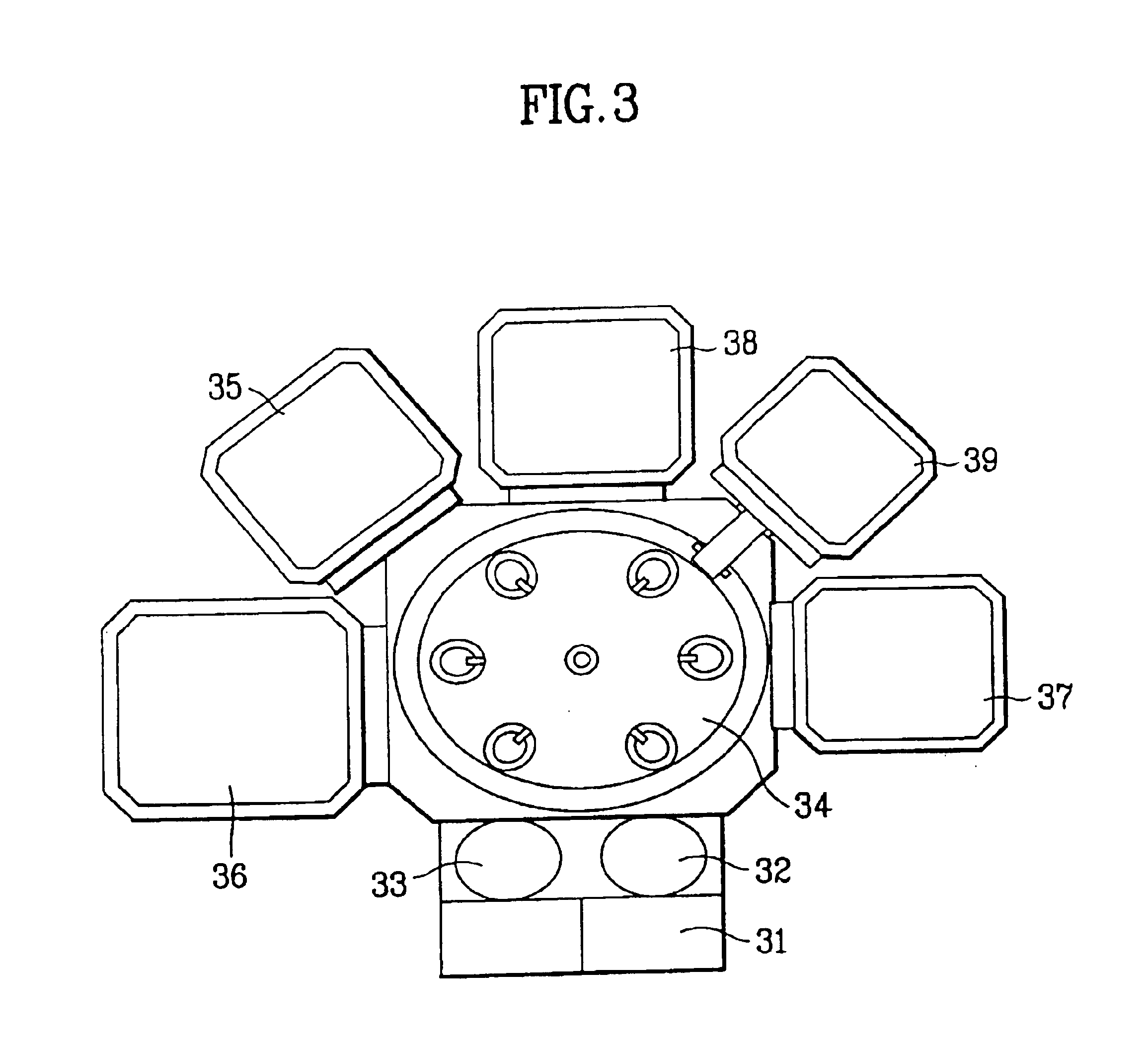
FIG. 3 is a plan view of a Cu film deposition equipment structure according to a third embodiment of the present invention. As shown in FIG. 3, the Cu film deposition equipment of the present invention includes a load lock 31 carrying out the steps before and after wafer (not shown) processes, an aligner 32 carrying out alignment so that the wafer reaches a desired position, and a de-gas and in-situ annealing chamber 33 removing residue such as gas produced on a surface of the wafer and processing in-situ annealing to enhance adhesion and to control texture. A feeding chamber 34 provided with a robot places the wafer in / out of each chamber.

The Cu film deposition equipment also includes a pre-cleaning chamber 35 cleaning the inside and the outside of a pattern using plasma on the wafer fed by the feeding chamber 34, a barrier metal deposition chamber 36 depositing barrier metal on the pre-cleaned wafer by PVD, CVD, or ALD process, a CE treatment chamber 37 processing an equal CE adso...


PUM

PropertyMeasurementUnit
temperatureaaaaaaaaaa
adhesionaaaaaaaaaa

Abstract

A Cu thin film deposition equipment of a semiconductor device is disclosed for improving deposition speed of a Cu thin film and lowering its corresponding cost. This equipment includes a load lock carrying out the steps before and after wafer processes, an aligner carrying out alignment so that a wafer reaches a desired position, a de-gas chamber removing residue such as gas produced on a surface of a wafer, and a feeding chamber provided with a robot placing the wafer in / out of each chamber. A pre-cleaning chamber cleaning the inside and the outside of a pattern using plasma on a wafer fed by the feeding chamber, a barrier metal deposition chamber, an adhesion glue layer (AGL) flash Cu deposition chamber, a CECVD deposition chamber, and a plasma treatment chamber are also provided with the equipment.

Description

BACKGROUND OF THE INVENTION1. Field of the InventionThe present invention relates to deposition equipment for a semiconductor device, and more particularly, to Cu film deposition equipment for a semiconductor device that enables catalyst deposition according to a chemical enhancer (CE) treatment and a plasma treatment for an equal super-filling.2. Description of the Background ArtWith the enhanced performance of semiconductor memory devices, increases in speed and reliability of semiconductor devices are major concerns for designers. Current Cu linings, which are used to increase the speed and reliability of semiconductor devices, use electroplating as a deposition method. However, the electroplating deposition method requires a thin film deposition process of a clean and safe Cu seed layer. Accordingly, the electroplating method depends highly on the seed layer and may be limited in a Tech level of 0.1 μm.Therefore, it is advantageous to use a metal organic chemical vapor depositio...

Claims


Application Information

Patent Timeline
Patent Type & Authority Patents(United States)
IPC IPC(8): H01L21/70H01L21/00H01L21/768C23C16/02H01L21/02H01L21/205H01L21/285
CPCH01L21/67167H01L21/67184H01L21/67207H01L21/76843H01L21/76864H01L21/76876H01L21/76877H01L21/76862H01L2221/1089
Inventor PYO, SUNG GVUKIM, SI BUM
Owner SK HYNIX INC
Why Eureka
Try Eureka