
Image forming method and image forming apparatus for suppressing movement of developer onto the electrostatic latent image carrier when the voltages applied to the charging and developing devices are raised or lowered

a technology developer, applied in the direction of electrographic process apparatus, corona discharge, instruments, etc., can solve the problems of wasting developer, wasting toner, wasting developer when the voltage applied to charging and developing devices is lowered, etc., and achieve the effect of suppressing the consumption of developer and reducing the number of image forming apparatus

Inactive Publication Date: 2005-01-18
MINOLTA CO LTD
View PDF5 Cites 11 Cited by
  • Summary
  • Abstract
  • Description
  • Claims
  • Application Information

AI Technical Summary

Benefits of technology

An object of the invention is to provide an image forming method, in which a charging device supplied with a charging voltage charges a surface of an electrostatic latent image carrier, image exposure is effected on a charged region of the surface of the electrostatic latent image carrier to form an electrostatic latent image, and a developing device supplied with a developing bias voltage develops the electrostatic latent image, and particularly to provide an image forming method, in which parts of an image forming apparatus can be reduced in number and consumption of developer can be suppressed.
Another object of the invention is to provide an image forming apparatus including an electrostatic latent image carrier, a charging device, a developing device and others for forming an image by charging a surface of the electrostatic latent image carrier by the charging device supplied with a charging voltage, effecting image exposure on a charged region of the surface of the electrostatic latent image carrier to form an electrostatic latent image, and developing the electrostatic latent image by the developing device supplied with a developing bias voltage, and particularly to provide an image forming apparatus, which allows reduction of the number of required parts, and can suppress consumption of developer.
According to the image forming methods and the image forming apparatus described above, the power source common to the charging device and the developing device is employed as the power sources for applying the charging voltage and the developing bias voltage to the charging device and the developing device, respectively. Therefore, the parts in the image forming apparatus can be reduced in number, and therefore the image forming apparatus can have reduced sizes.
Accordingly, it is possible to suppress wasting of the developer when raising and / or lowering the voltages applied to the charging and developing devices.
According to this image forming apparatus, the fully exposed surface portion of the electrostatic latent image has a surface potential lowered nearly to a grand potential. Accordingly, the power source output control portion stops the output from the power source at the same time as this surface portion reaches the developing position opposed to the developing device, and thereby stops the voltage application to the developing device so that movement of the developer from the developing device onto the electrostatic latent image carrier is suppressed. Simultaneously with the stop of voltage application to the developing device, or after the stop of the voltage application and before completion of passing of the fully exposed surface portion through the developing position, and in other words, before a trailing portion, which may be charged in some cases depending on the manner of fully exposing processing, of the fully exposed portion of the electrostatic latent image carrier reaches the developing device, the electrostatic latent image carrier is stopped so that the movement of the developer from the developing device onto the electrostatic latent image carrier is suppressed. This suppresses wasting of the developer. For example, in reversal development with two-component developer, consumption of carrier can be suppressed.
The invention can also achieve the following advantage. As compared with a structure including independent power sources for applying voltages to the charging device and the developing device, respectively, it is possible to reduce variations, which may occur in potential difference between an image background potential of the electrostatic latent image carrier and the voltage applied to the developing device when the image forming apparatuses are manufactured, so that designing of the developer and the developing system can be easy.

Problems solved by technology

As a result, developer moves onto the electrostatic latent image carrier when the voltages applied to the charging device and the developing device are raised so that the developer is wasted.
The developer is likewise wasted when the voltages applied to the charging and developing devices are lowered.
This wastes the toner.
This wastes the carrier.
For example, in an image forming apparatus, which perform reversal development of an electrostatic latent image with a one-component developer primarily made of negatively chargeable toner, negatively charged toner moves onto a region of the electrostatic latent image carrier, which is not yet charged, when the voltages applied to the charging and developing devices are raised so that the toner is wasted.

Method used


Image

  • Image forming method and image forming apparatus for suppressing movement of developer onto the electrostatic latent image carrier when the voltages applied to the charging and developing devices are raised or lowered
  • Image forming method and image forming apparatus for suppressing movement of developer onto the electrostatic latent image carrier when the voltages applied to the charging and developing devices are raised or lowered
  • Image forming method and image forming apparatus for suppressing movement of developer onto the electrostatic latent image carrier when the voltages applied to the charging and developing devices are raised or lowered

Examples


first embodiment

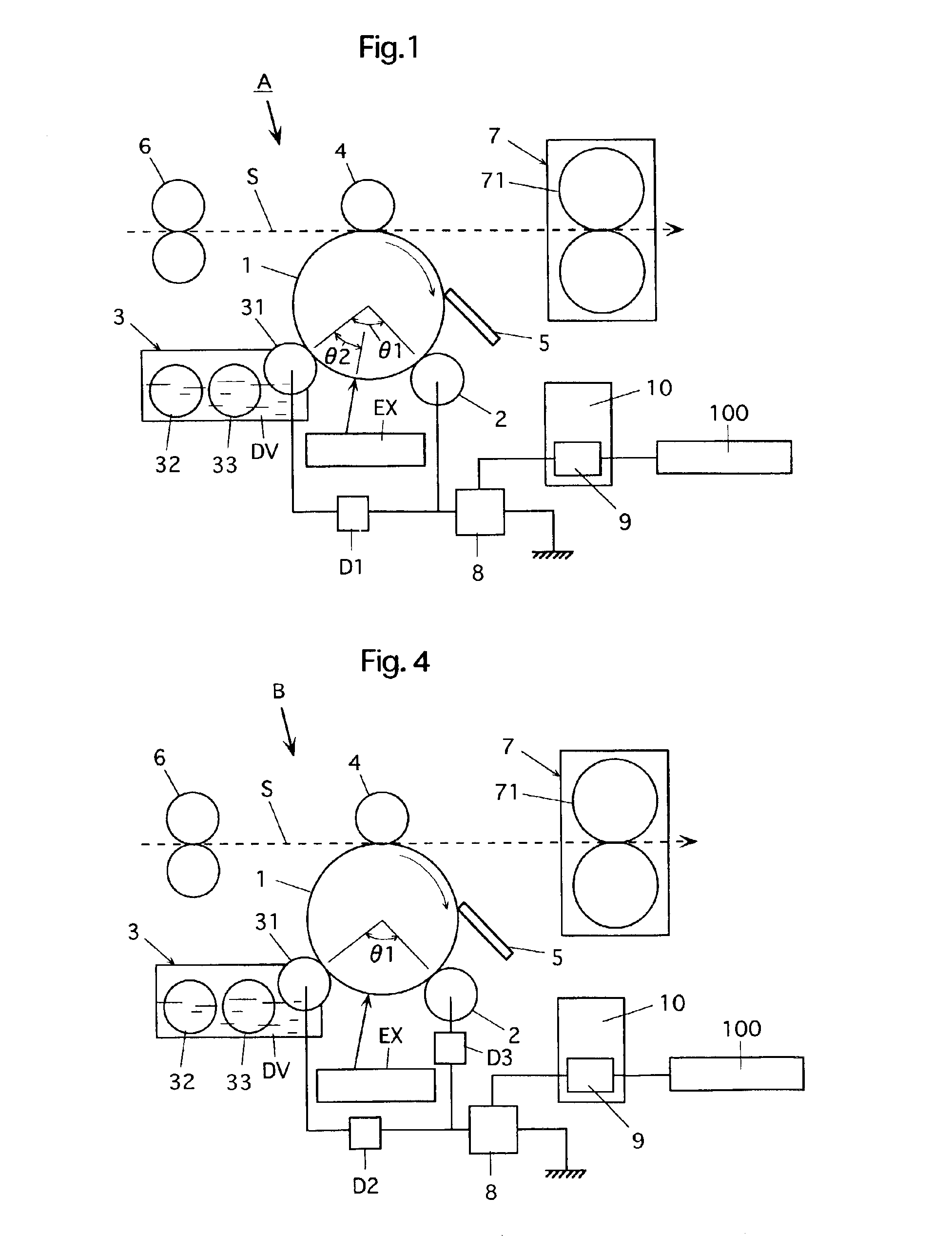
FIG. 1 shows a schematic structure of an electrophotographic image forming apparatus (printer) of a first embodiment of the invention.

An image forming apparatus A has a rotatable drum-like photosensitive member 1 serving as an electrostatic latent image carrier, and also includes a charging roller 2 serving as a charging device, a developing device 3, a transfer roller 4 serving as a transfer device, and a cleaning device 5 formed of a cleaning blade, which are arranged in this order around the photosensitive member 1. In FIG. 1, an image exposing device EX of a laser beam type is arranged under the photosensitive member 1. In FIG. 1, a timing roller pair 6 and a fixing device 7 are arranged on the left and right sides of the transfer roller 4, respectively.

The developing device 3 has a developing roller 31 opposed to the photosensitive member 1 as well as rotary members 32 and 33 for stirring and applying developer, and accommodates two-component developer DV containing a negativel...

second embodiment

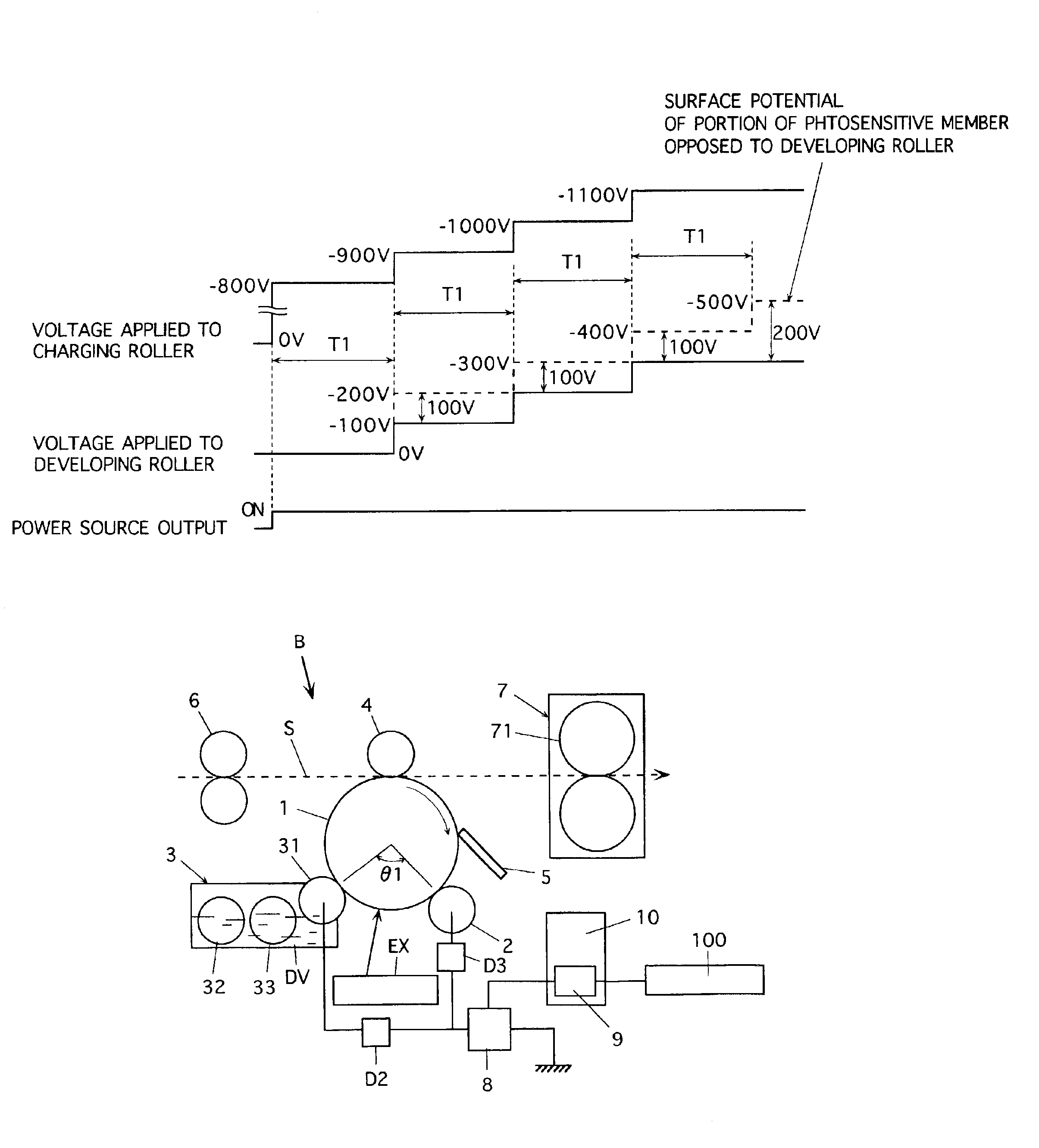
FIG. 4 shows a schematic structure of an image forming apparatus B of a second embodiment.

The apparatus B differs from the apparatus A shown in FIG. 1 in that a Zener diode D2 lowering a voltage by 700 V is employed as the voltage changing device instead of the Zener diode D1, and a voltage changing element D3 raising a voltage by 100 V is connected between the power source 8 and the charging roller 2. The image forming apparatus B has the same structure as the apparatus A except for the above, and performs the image forming operation basically in the same manner as the apparatus A. The same parts as those in the apparatus A bear the same reference numbers or symbols.

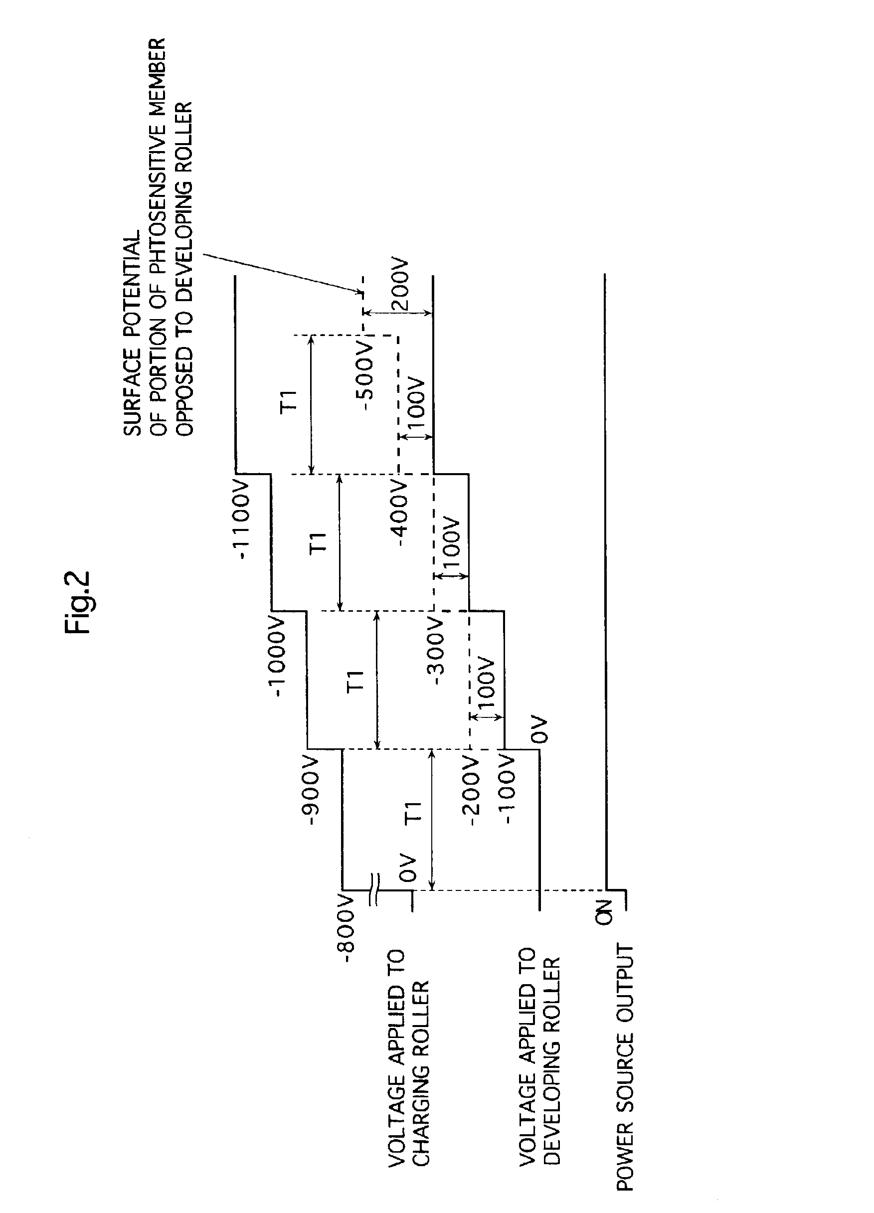
In the image forming apparatus B, when the voltages applied to the charging and developing rollers 2 and 31 are to be raised, the control portion 9 controls the power source 8 to start the supply of the voltages of −700 V, to raise the applied voltages by 100 V upon every elapsing of the time T1 and to supply finally th...

third embodiment

An image forming apparatus of a third embodiment has basically the same structure as the image forming apparatus A shown in FIG. 1, and performs the image formation basically in the same manner as the apparatus A. The voltages applied to the charging and developing rollers 2 and 31 are raised as illustrated in FIG. 2. However, the voltages applied to the charging and developing rollers 2 and 31 are lowered as illustrated in FIG. 5. Thus, the control portion 9 controls the output of the power source 8 to perform the lowering as illustrated in FIG. 5.

As illustrated in FIG. 5, the ending operation starts after completion of the image forming operation.

In this ending operation, a surface portion of the photosensitive member 1, and particularly the surface portion extending across the surface traveling direction is fully exposed to the full exposing light of the image exposing device EX. A time T2 is required before the fully exposed surface portion of the photosensitive member 1 reaches...


PUM


Abstract

An electrophotographic image forming apparatus having a photosensitive member 1, a charging roller 2 and a developing roller 31, and including an output variable power source 8 common to the charging and the developing rollers 2 and 31 for applying voltages to the charging and developing rollers 2 and 31, respectively, a power source output control portion 9, and a voltage changing device (Zener diode D1) interposed between the developing roller 31 and the power source 8, wherein, when the voltages applied to the charging and developing rollers 2 and 31 are raised to and lowered from voltages required for image formation, respectively, the control portion 9 controls an output of the power source 8 to perform the raising and lowering of the applied voltages for a predetermined time while keeping a potential difference for suppressing movement of developer onto the photosensitive member 1 between the voltages applied to the charging and developing rollers 2 and 31.

Description

CROSS-REFERENCE TO RELATED APPLICATIONThis application is based on Japanese patent application No. 2002-248292 filed in Japan on Aug. 28, 2002, the entire content of which is hereby incorporated by reference.BACKGROUND OF THE INVENTION1. Field of the InventionThe present invention relates to an electrophotographic image forming apparatus of a stand-alone type, a network type or the like for forming monochrome images and / or color images such as a copying machine, a printer, a facsimile machine or a composite machine including a combination of two or more of them.2. Description of Related ArtThe above kind of image forming apparatus in the prior art includes an electrostatic latent image carrier, a charging device and a developing device, and further includes a charging power source or supply for charging a surface of the electrostatic latent image carrier to a predetermined potential and a developing bias power source for applying a developing bias voltage to the developing device fo...

Claims


Application Information

Patent Timeline
IPC IPC(8): G03G15/00G03G15/02G03G21/00G03G15/06
CPCG03G15/5004G03G15/80G03G2221/0005
Inventor TAKAI, TAKAYUKI
Owner MINOLTA CO LTD
Learn More