Eureka AIR delivers breakthrough ideas for toughest innovation challenges, trusted by R&D personnel around the world.

Radiation sensor device

a sensor device and radiation sensor technology, applied in the field of radiation imaging systems, can solve the problems of difficult to achieve sufficient resolution, easy damage to semiconductor surfaces by x-rays or mev photons, radiation sensitive, etc., and achieve the effect of improving image resolution, simple and comparatively inexpensive manufacturing

Inactive Publication Date: 2005-01-11
C RAD IMAGING AB
View PDF7 Cites 25 Cited by
  • Summary
  • Abstract
  • Description
  • Claims
  • Application Information

AI Technical Summary

Benefits of technology

"The present invention provides an improved radiation sensor device with a large number of individually connected radiation sensitive elements. The device has improved image resolution and is simple and inexpensive to manufacture. The sensor device uses the edge portion of a circuit board as an area for radiation sensing, and each circuit board has a row of radiation sensitive elements connected to signal processing means located outside the radiation field. The signal processing means includes amplifiers and multiplexers in ASICs, which can be located on the same circuit board or different heights to maximize space utilization. The radiation sensitive elements can be charge collectors, U-shaped pixels, flat sensor cells, or radiation sensitive elements formed by the end surfaces of connection lines. The sensor surface can be planar or curved. The invention offers the advantage of having a large number of radiation sensitive elements, improved image resolution and contrast, integrating electronic readout without charge transfer between pixels, avoiding irradiation of semi-conductor devices, and a straight-forward design."

Problems solved by technology

This makes it extremely difficult to achieve sufficient resolution and integrating electronic readout is generally required.
A major problem associated with CCDs and similar devices is the fact that they are very radiation sensitive and the semiconductor surface easily get damaged by X-rays or MeV photons.
Such devices are hence not a practically feasible alternative for systems with high charge flow rates.
However, radiation-resistant transistors are extremely difficult to achieve, making the solution with plates of amorphous silicon and selenium rather problematic.
Moreover, such plates are very expensive and provide a comparatively slow readout.
Previous attempts to accomplish a sufficiently large surface area by means of this technology have not succeeded.
Due to complicated electronic structure, implementation of such a solution is generally not practically feasible when the number of pixels grows.
Besides being inflexible and bulky when a large number of sensitive elements, and thus a large number of horizontal matrixes, are needed, the proposed solution excludes realizations with planar or smooth sensor matrix surfaces.
This is achieved by a comparatively complicated design, where each sensitive element comprises an electric switch and switching lines and read lines are provided at rows and columns, respectively, of the matrix.
From the above discussion, it follows that such a solution is comparatively radiation sensitive.
None of the above-cited documents discloses a radiation resistant sensor device presenting a large pixel area.
The existing radiation sensor devices are associated with severe drawbacks and limitations and there is a considerable need for an improved radiation sensor device offering efficient readout and improved imaging even at high charge-flow rates.

Method used


Image

  • Radiation sensor device
  • Radiation sensor device
  • Radiation sensor device

Examples


Embodiment Construction

Throughout the following description similar or corresponding elements bear the same reference numbers. The term “radiation” comprises electromagnetic radiation, such as visible light, as well as particle radiation including radiation of charged particles, e.g. electrons, and uncharged particles, e.g. neutrons.

Many radiation systems of today require read-out units with a comparatively large number of radiation sensitive elements. Integrating electronic readout may often be the only practically feasible alternative, in particular at high charge-flow rates. As mentioned, it would hereby be desirable to couple certain read-out electronics, such as a charge amplifier and / or a multiplexer, to each pixel. Then severe prior-art problems would be avoided, since charges would not have to be moved in a controlled manner on a special surface, nor would radiation sensitive elements, like transistors, have to be arranged at the pixels. However, such an implementation implies one amplifier and / or...


PUM


Abstract

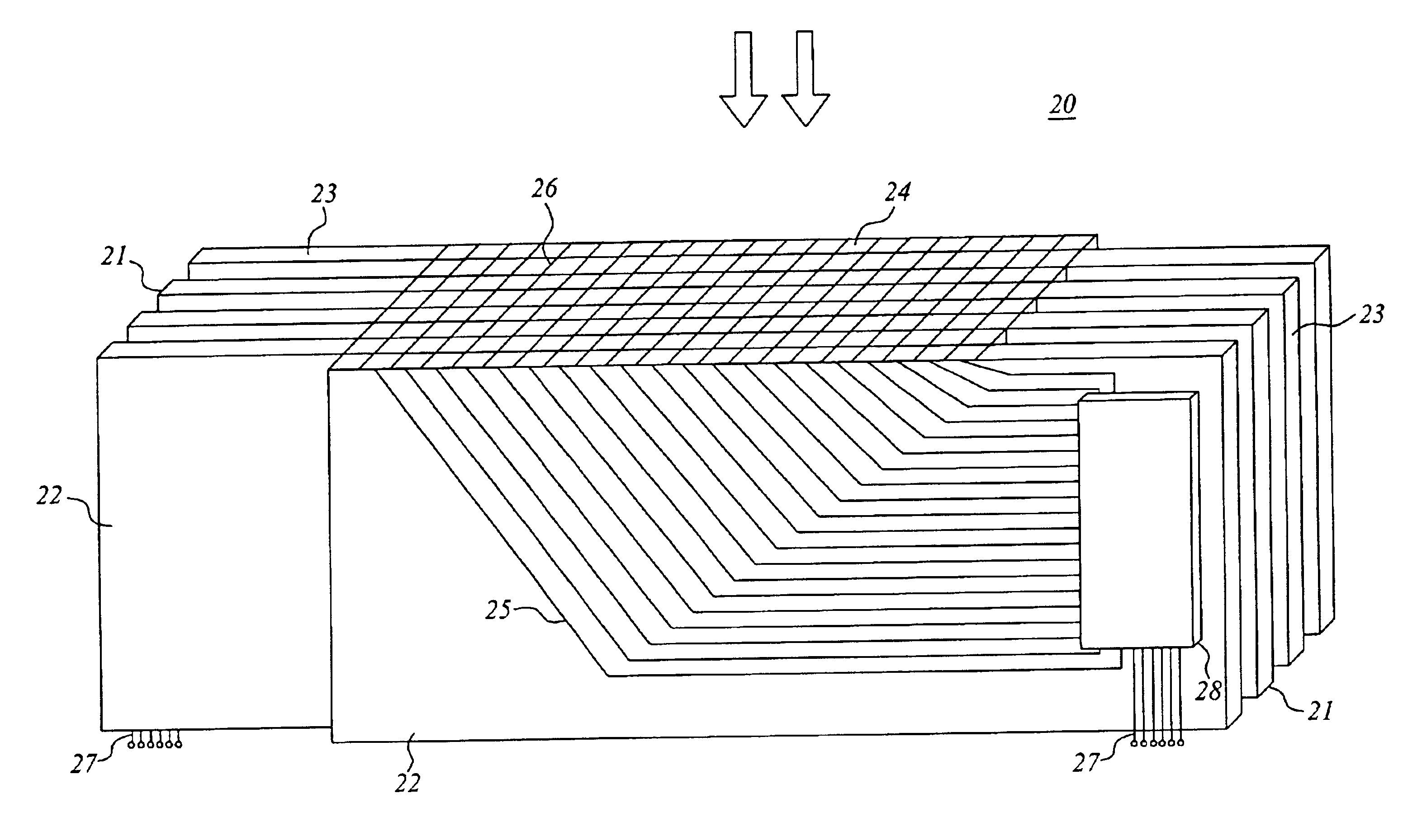
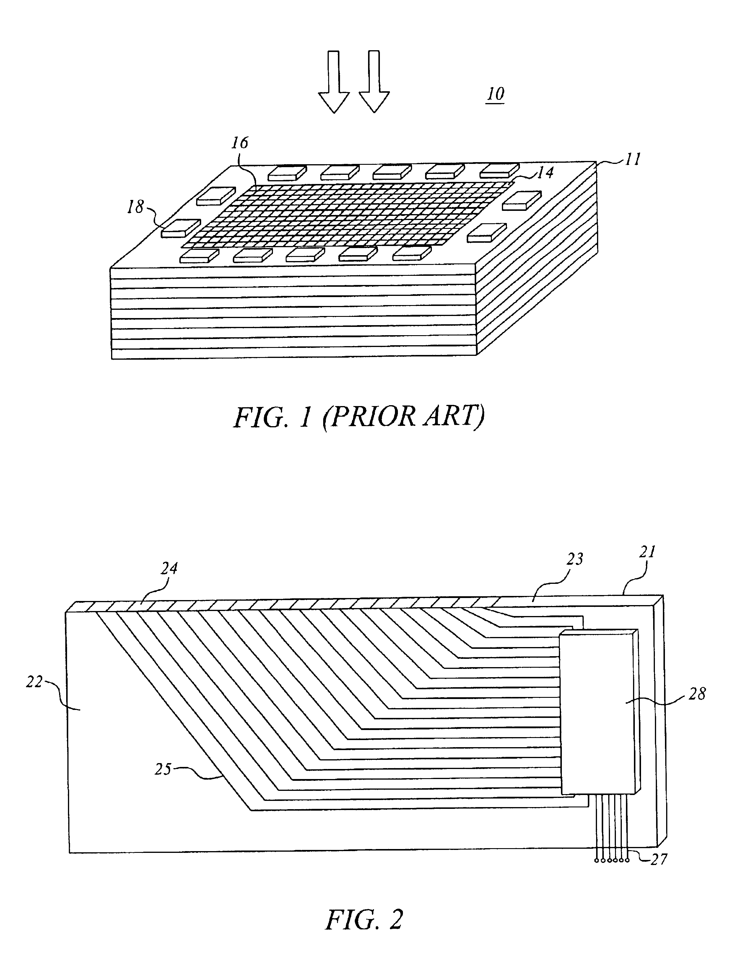
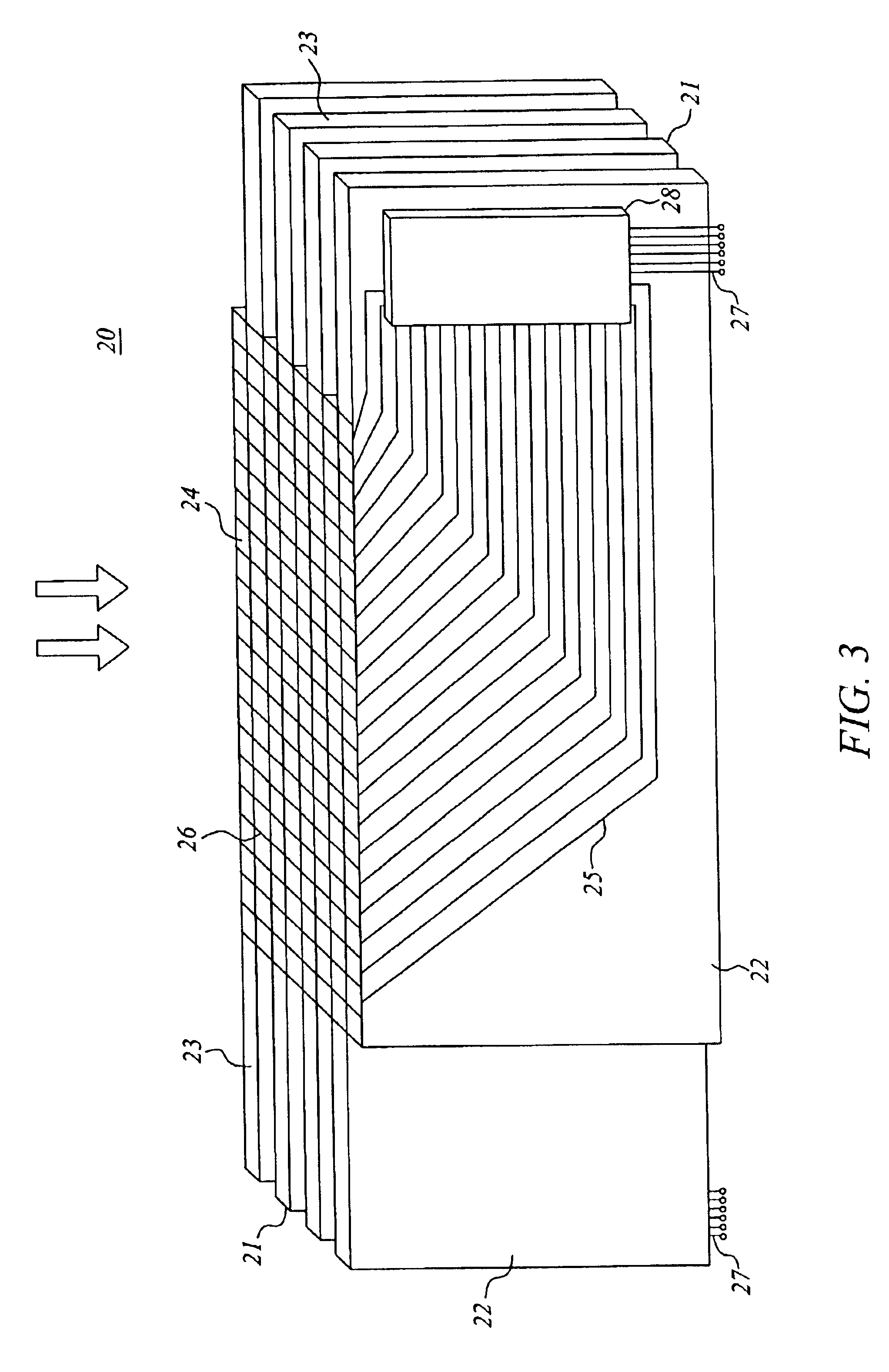
A radiation sensor device (20) for detection of radiation. A sensor device with an array of radiation sensitive elements (24) forming a sensor surface (26) is provided. The device comprises a number of circuit boards (21), each with a row of radiation sensitive elements, such as X-ray sensitive charge collectors, provided at the edge portion. The radiation sensitive elements are each connected to signal processing means (28), e.g. ASICs with amplifiers, outside the radiation field by a respective connection line (25) arranged on a main surface (22) of the circuit board. A number of circuit boards are arranged adjacent to each other with the main planes substantially perpendicular to the sensor surface. By using the circuit card depth the invention easily provides surfaces with a very large number of individually connected radiation sensitive elements, resulting in improved image resolution.

Description

TECHNICAL FIELDThe present invention relates to radiation imaging systems and more specifically to a radiation sensor device used for detection of radiation.BACKGROUNDRadiation sensor devices are used to detect radiation and provide spatial mapping of radiation intensity in radiation-based imaging systems. Such systems involve detection of incoming radiation, such as X-rays, gamma photons and charged particles, in a wide range of different applications including medical applications. Basically, a radiation source generates a beam in the direction of an object to be examined and a detector measures the intensity of the beam after it has passed through the object. The sensor device detects and measures the information required to produce an image representing the attenuation of the radiation resulting from absorption and scattering by the structure through which the beam traveled.The sensor device is generally located within the detector unit and comprises a number of radiation sensit...

Claims


Application Information

Patent Timeline
Patent Type & Authority Patents(United States)
IPC IPC(8): G01T1/00G01T1/185G01T1/24
CPCG01T1/24
Inventor BRAHME, ANDERSIACOBAEUS, CHRISTIANOSTLING, JANINAKIHLBERG, ROGER
Owner C RAD IMAGING AB
Why Eureka
Eureka Blog
Learn More