
Dual stage level shifter for low voltage operation

a level shifter and dual stage technology, applied in logic circuits, pulse automatic control, pulse technique, etc., can solve the problems of limiting the range of acceptable input and output voltages, unable to operate at very low voltages, and limited voltage rang

Inactive Publication Date: 2005-01-04
XILINX INC
View PDF10 Cites 33 Cited by
  • Summary
  • Abstract
  • Description
  • Claims
  • Application Information

AI Technical Summary

Benefits of technology

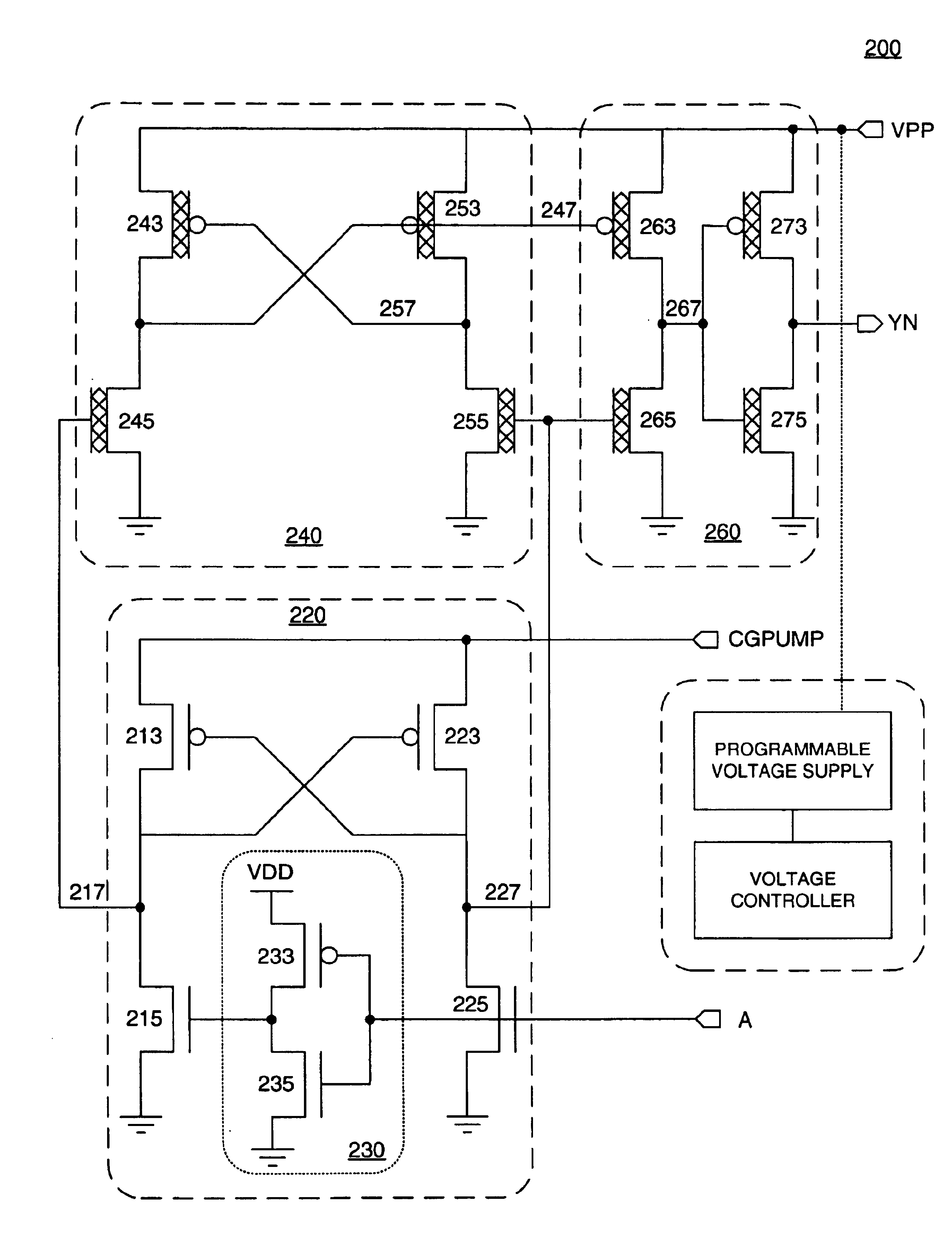
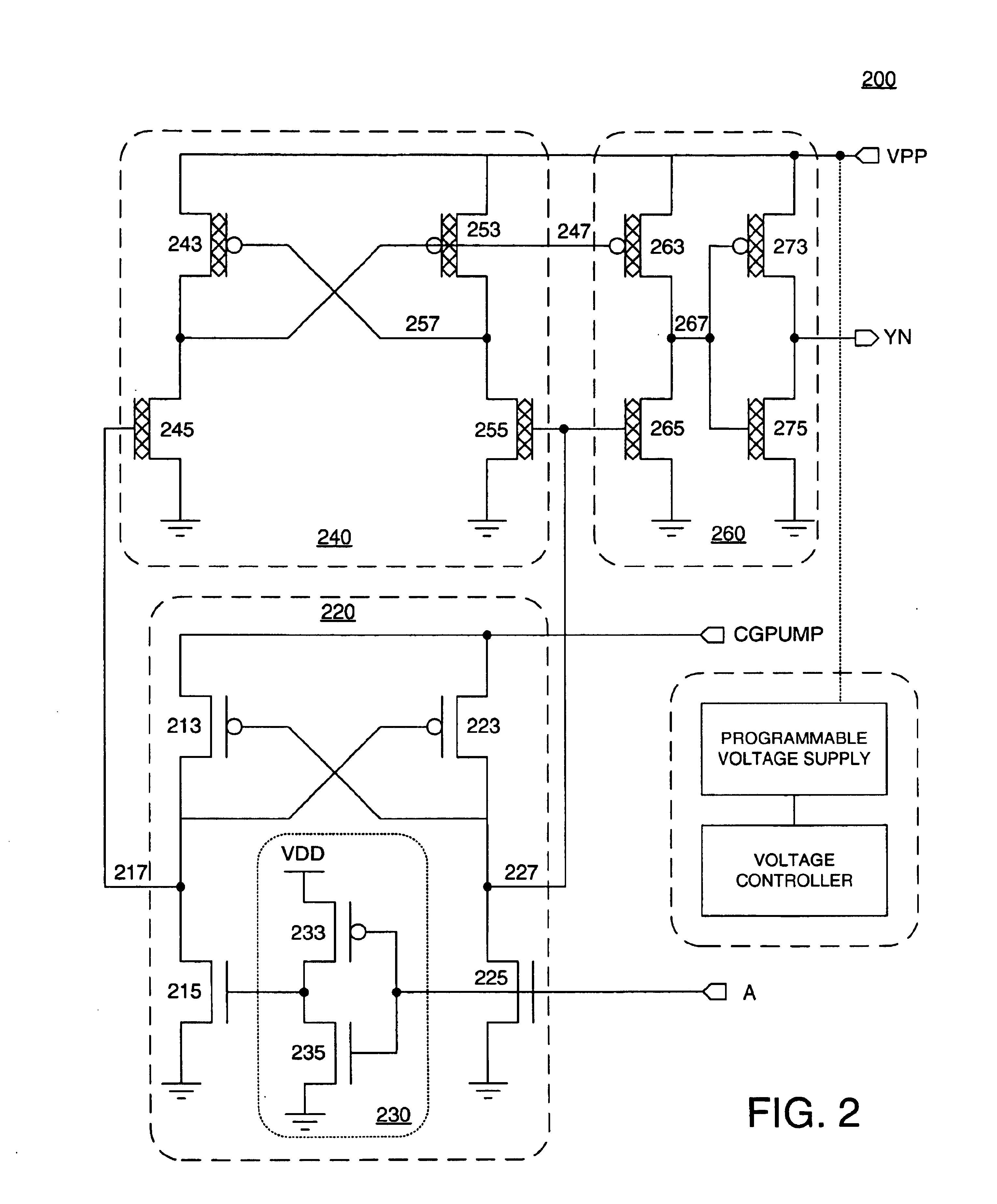
In accordance with the present invention, a level shifting circuit includes two stages. The first stage shifts an input signal to an intermediate voltage level, and the second stage shifts the intermediate voltage level to an output voltage level. The intermediate voltage level is designed to be at a level within the safe operating ranges of the first and second stages. For instance, the intermediate voltage level can be designed to be below the maximum voltage tolerable by the first stage, and above the minimum voltage for functionality of the second stage. This enables the level shifter to function at very low input voltages and over a wide range of output voltages. In one embodiment, each stage of the level shifter comprises a pair of cross-coupled PMOS transistors and a pair of input NMOS transistors. In some embodiments, the level shifter further includes an output buffer stage.

Problems solved by technology

One challenge in designing integrated circuits (ICs) is accommodating several different power supply voltages on a single IC.
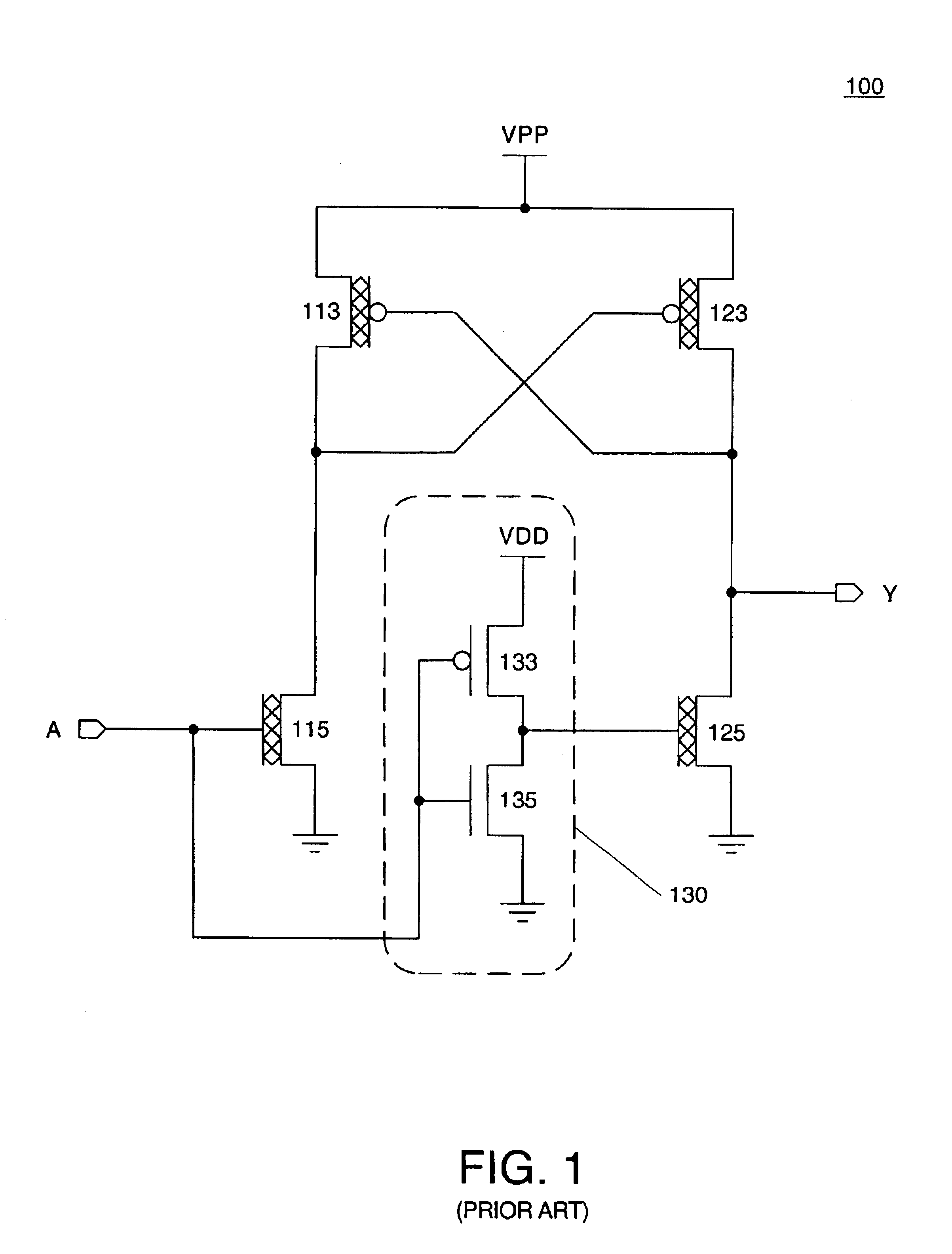
One problem associated with prior art level shifters is that they only operate over a limited range of voltages.
Limitations in process technology can restrict the range of acceptable input and output voltages for a level shifter.
However, the high voltage transistors also have high threshold voltages, and therefore cannot operate at very low voltages.
As minimum feature sizes shrink, the correspondingly decreasing core voltages only exacerbate this problem.

Method used


Image

  • Dual stage level shifter for low voltage operation
  • Dual stage level shifter for low voltage operation
  • Dual stage level shifter for low voltage operation

Examples


Embodiment Construction

The present invention is believed to be applicable to a variety of integrated circuits and systems. The present invention has been found to be particularly applicable and beneficial for certain nonvolatile memory circuits. While the present invention is not so limited, specific examples and details for nonvolatile memory circuits are set forth to provide a more thorough understanding of the present invention. However, it will be apparent to one ordinarily skilled in the art that the present invention can be practiced without these specific details, and can be practiced within other architectural variations.

FIG. 2 shows a circuit diagram of a level shifter 200 in accordance with the present invention. Level shifter 200 includes a first stage 220 and a second stage 240. Input A of level shifter 200 is configured to receive a low voltage input signal. The low voltage input signal is shifted to a high voltage output signal at node 247 of level shifter 200. As shown in FIG. 2, the input ...


PUM


Abstract

A level shifter for low voltage operation includes two level shifting stages. The first stage shifts the input voltage level to an intermediate voltage level, and the second stage shifts the intermediate voltage level to an output voltage level. This two-stage arrangement allows the level shifter to function for very low input voltages, and enables functionality across a wide range of output voltages. The first stage is designed to be compatible with very low input voltages and the intermediate voltage level is chosen to be within the safe operating limits of the first stage. The intermediate voltage level is also high enough to drive the high voltage devices of the second stage. This level shifter can be used where multiple output voltage levels are required depending on the particular application or operating mode.

Description

FIELD OF THE INVENTIONThe invention relates to integrated circuits, and, more particularly, to level shifters.BACKGROUND OF THE INVENTIONOne challenge in designing integrated circuits (ICs) is accommodating several different power supply voltages on a single IC. Typically, an IC will have a “core” power supply for powering the bulk of its internal circuitry. The voltage level of the core power supply is usually kept low in order to conserve power. As IC fabrication processes improve and the minimum feature size on an IC decreases, the allowable core voltage also decreases. ICs fabricated using current IC processes can typically operate at approximately 1.0V, and even lower voltages will be possible soon, as process technology continues to improve.For particular applications, however, an IC can require the use of one or more other voltage levels, usually higher than the core voltage. For example, an IC may need to communicate with other components in a system using an input / output (I...

Claims


Application Information

Patent Timeline
IPC IPC(8): H03K3/356H03K3/00
CPCH03K3/356113
Inventor DAVIES, JR., THOMAS J.
Owner XILINX INC
Learn More