Gaseous-based radiation detector
a technology of ionizing radiation and detectors, which is applied in the field of gaseous-based ionizing radiation detectors, can solve the problems of inacceptability, large and bulky detectors, and harm to detectors, and achieves the effects of reducing the cost of detectors, and reducing the cost of ionizing radiation detection
- Summary
- Abstract
- Description
- Claims
- Application Information
AI Technical Summary
Benefits of technology
Problems solved by technology
Method used
Image
Examples
first embodiment
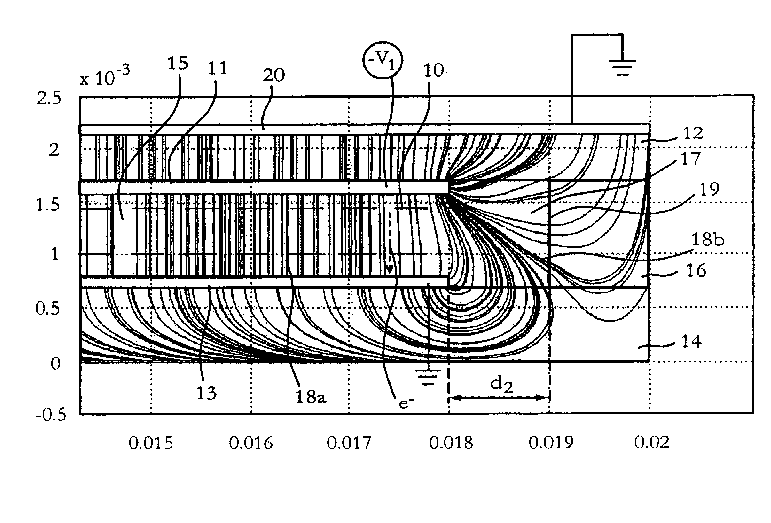
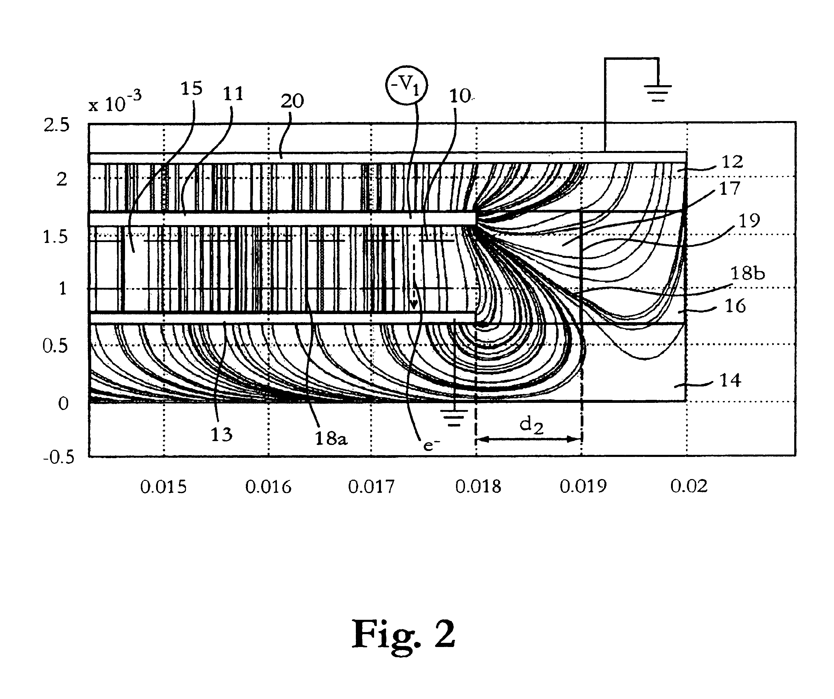
FIG. 2 is a front view of an end portion of a detector for planar beam radiography according to the present invention.
The detector is oriented such that a planar X-ray beam can enter sideways between a cathode arrangement 11, 12 and an anode arrangement 13, 14. A radiation transparent slit window (schematically indicated by dashed line 10), and optionally a collimator window (not illustrated) are provided at the front of the detector to form an entrance for the X-ray beam to the detector.
Each of the electrode arrangements includes an electrically conducting electrode layer 11, 13 supported by a respective dielectric substrate 12, 14, wherein the arrangements are oriented such that the cathode 11 and anode 13 layers are facing each other.
Preferably, the electrode arrangements 11, 12 and 13, 14 are planar, rectangular and parallel to each other. However, other geometries may be employed.
The electrode arrangements are separated by a spacer or support 16 along at least portions of the p...
second embodiment
Turning now to FIG. 3, which schematically illustrates in a front view a portion of a modified radiation detector the present invention will shortly be depicted.
This detector differs from the FIG. 2 detector only in that a further electrically conducting layer 21 is arranged on a surface of the dielectric anode substrate 14, which is opposite to the surface that carries the anode layer 12. The electrically conducting layer 21 is as layer 20 grounded, and this affects the electric field particularly within the dielectric anode substrate 14, see the illustrated electric field lines in FIG. 3. The electric field within the inter-electrode space close to the spacer 16 is similar to the one in FIG. 2.
third embodiment
In FIG. 4 is schematically illustrated in a front view a portion of yet a modified radiation detector and this third embodiment of the detector differs from the FIG. 2 embodiment only as regards the extension of the electrically conducting layer 20. The layer, in FIG. 4 denoted 20', extends above the cathode layer 11 and beyond the outer periphery of the cathode layer 11 by a distance d.sub.3 as indicated. Distance d.sub.2 indicates, as in FIG. 2, the distance between the inner surface of the spacer 16 and the outer peripheries of the electrode layers 11, 13. Thus, the electrically conducting layer 20' extends beyond also the inner surface of the spacer 16.
PUM
 Abstract
Description
Claims
Application Information
 - R&D
- Intellectual Property
- Life Sciences
- Materials
- Tech Scout
- Unparalleled Data Quality
- Higher Quality Content
- 60% Fewer Hallucinations
Browse by: Latest US Patents, China's latest patents, Technical Efficacy Thesaurus, Application Domain, Technology Topic, Popular Technical Reports.
© 2025 PatSnap. All rights reserved.Legal|Privacy policy|Modern Slavery Act Transparency Statement|Sitemap|About US| Contact US: help@patsnap.com


