
Glitcher system and method for interfaced or linked architectures

a technology of interfaced or linked systems and interfaces, applied in the direction of digital signal error detection/correction, instruments, recording signal processing, etc., can solve the problems of device(s) being completely or completely shut down or killed, the simulation of a noisy interface or dirty link between interfaced or linked devices coupled together by an interfaced or linked architecture is extremely difficult, and the unplugging of the link is very unpredictabl

Inactive Publication Date: 2003-12-02
GOOGLE LLC
View PDF10 Cites 5 Cited by
  • Summary
  • Abstract
  • Description
  • Claims
  • Application Information

AI Technical Summary

Benefits of technology

It is therefore one object of the present invention to provide a system and method that allows for verification of error recovery by an interfaced or linked architecture system.
It is another object of the present invention to provide accurate, reliable, and more assured fault simulation, such as noisy interface and dirty link simulations, within an interfaced or linked architecture system for verification of such error recovery.
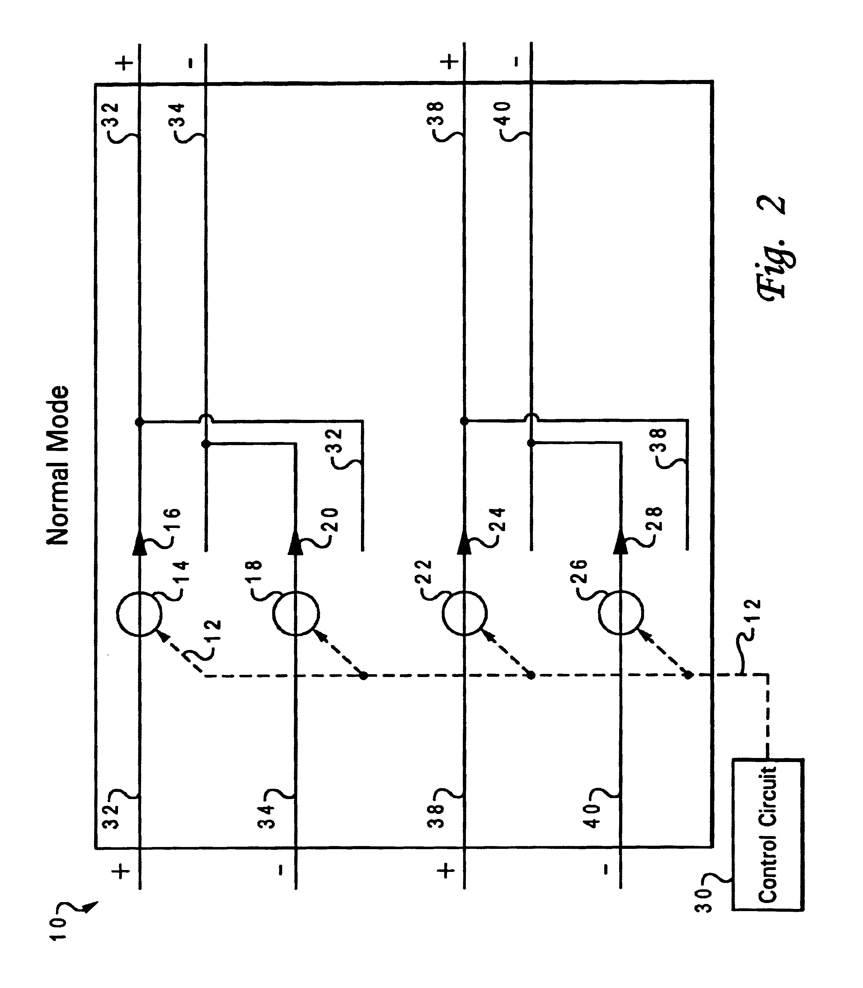
The foregoing objects are achieved as is now described. A serial differential link glitcher system and method which allow for verification of error recovery by an interfaced or linked architecture system. The system and method provide accurate, reliable, and more assured fault simulation, such as noisy interface and dirty link simulations, within an interfaced or linked architecture system for verification of such error recovery and verifies and checks data at a lower level between interfaced devices. The system and method verify disparity errors between interfaced devices and also perform verification of error recovery between electrically linked devices or optically linked devices. At least two devices are coupled together by communication lines. Normal mode allows for normal operation of and normal communication between the at least two devices, and glitch mode provides fault simulation and disparity errors and phase inversion between the at least two devices for testing error recovery of the system. Proper polarity of the communication lines is maintained between the at least two devices when the system is in normal operation mode. The polarity of the communication lines between the at least two devices is switched and inverted when the system is in glitch mode wherein phase inversion and disparity errors in the communication lines are created. The glitcher switch system comprises a switch and a control circuit. The switch allows switching between the communication mode, that is, between the normal operation mode and the glitch mode. The control circuit controls the switch in placing the system in the normal operation mode or the glitch mode.

Problems solved by technology

However, simulation of a noisy interface or dirty link between interfaced or linked devices that are coupled together by an interfaced or linked architecture has been extremely difficult, especially at high speeds, in order to verify and test the error recovery performance of the interfaced or linked architecture system.
However, the results of unplugging a link or using a faulty or bad cable between devices is very unpredictable.
Typically, the unplugging of a link or the using of a faulty or bad cable between the devices may result in either the device(s) being entirely or completely shut down or killed wherein fault simulation and error recovery testing cannot be continued or may result in no errors being generated wherein accurate fault simulation and error recovery testing cannot be achieved.

Method used


Image

  • Glitcher system and method for interfaced or linked architectures
  • Glitcher system and method for interfaced or linked architectures
  • Glitcher system and method for interfaced or linked architectures

Examples


Embodiment Construction

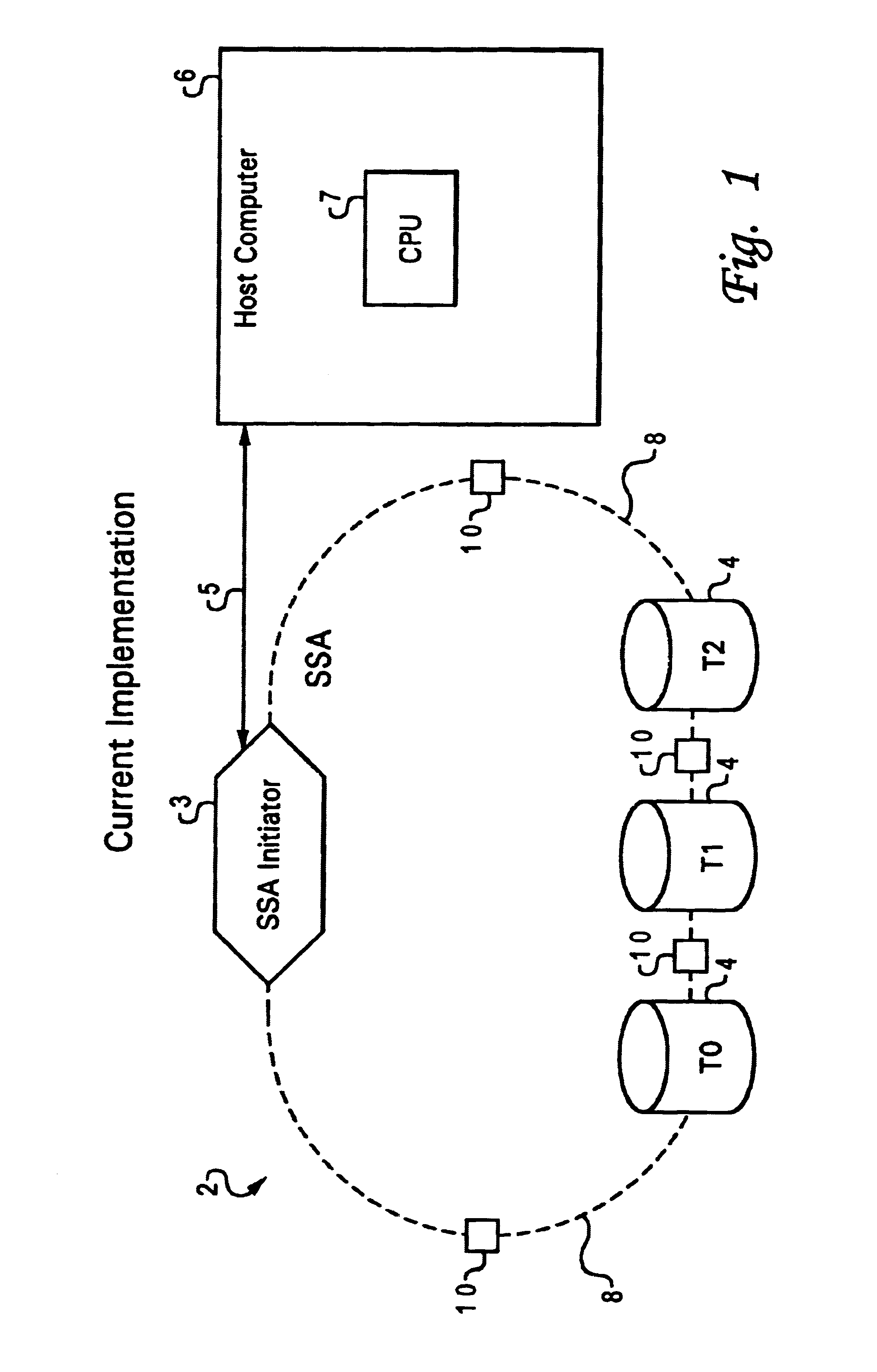
The present invention is a glitcher system 10 and method for interfaced or linked architectures. Interfaced or linked architectures generally include two main types: a serial differential interfaced system and an optical interfaced system. Examples of such interfaced or linked architectures include but are not limited to serial storage architecture (SSA) (serial differential interface type), fibre channel (optical type), IEEE 1394 interface architecture, ethernet, USB, and ATM. The present invention glitcher system 10 and method are not in any way limited to being used in the specific interfaced or linked architectures disclosed hereafter, and the present invention may be used or adapted to be used in any type of suitable interfaced or linked architecture.

The system 10 and method allow for verification of error recovery by an interfaced or linked architecture, such as a serial differential interfaced system or an optical interfaced system. The system 10 and method provide accurate, ...


PUM

PropertyMeasurementUnit
polarityaaaaaaaaaa
length of timeaaaaaaaaaa
electricalaaaaaaaaaa

Abstract

A serial differential link glitcher system and method which allow for verification of error recovery by an interfaced or linked architecture system. The system and method provide accurate, reliable, and more assured fault simulation, such as noisy interface and dirty link simulations, within an interfaced or linked architecture system for verification of such error recovery and verifies and checks data at a lower level between interfaced devices. The system and method verify disparity errors between interfaced devices and also perform verification of error recovery between electrically linked devices or optically linked devices. At least two devices are coupled together by communication lines. Normal mode allows for normal operation of and normal communication between the at least two devices, and glitch mode provides fault simulation and disparity errors and phase inversion between the at least two devices for testing error recovery of the system. Proper polarity of the communication lines is maintained between the at least two devices when the system is in normal operation mode. The polarity of the communication lines between the at least two devices is switched and inverted when the system is in glitch mode wherein phase inversion and disparity errors in the communication lines are created. The glitcher switch system comprises a switch and a control circuit. The switch allows switching between the communication mode, that is, between the normal operation mode and the glitch mode. The control circuit controls the switch in placing the system in the normal operation mode or the glitch mode.

Description

BACKGROUND OF THE INVENTION1. Technical FieldThe present invention relates in general to a glitcher for interfaced or linked systems and in particular to an interfaced or link glitcher system and method that creates faults and simulates noisy interfaces to verify error recovery in various interfaced or linked architectures.2. Description of the Related ArtVarious types of interfaced or linked architectures exist wherein various computer systems and / or devices are coupled together in communication with each other by these various types of interfaced or linked architectures. Two main types of interfaced or linked architectures are a serial differential interfaced system and an optical interfaced system. Examples of such interfaced or linked architectures include but are not limited to serial storage architecture (SSA) (serial differential interface type), fibre channel (optical type), IEEE 1394 interface architecture, ethernet, USB, and ATM.As an example, a serial storage architecture...

Claims


Application Information

Patent Timeline
Patent Type & Authority Patents(United States)
IPC IPC(8): G11B20/18
CPCG11B20/1816
Inventor EMBERTY, ROBERT GEORGEKLEIN, CRAIG ANTHONYWILLIAMS, GREGORY ALLEN
Owner GOOGLE LLC
Learn More